I wanted to take another moment to share a few thoughts about last night’s Project Night. Sometimes, when I’m speaking on the spot, everything I want to say doesn’t come to me all at once, so please bear with me again. I really was very impressed by the level of talent that was showcased. And, more importantly, I know there is even more of it out there amongst the folks who didn’t get the opportunity to present. But I hope you will during a future club meeting.
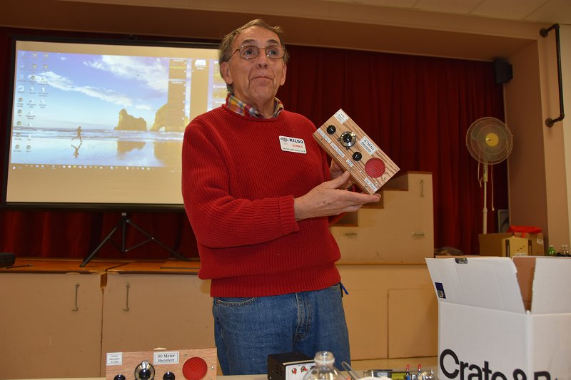
Dennis, K1LGQ Shows QRP Kits at Project Night
The Jan 2016 Project Night was my first Nashua Area RC meeting. And, it was that first meeting which played an instrumental role in sucking me completely into the hobby: and I’m in pretty deep right now.
I’ve noticed over my years on this pale, blue dot that part of my personality is to think big, try to generate a lot of ideas, but then sometimes get fearful to execute. I think it’s because I’m afraid to fail and I’ve convinced myself (probably through some poor advice by the few poor mentors I’ve had in my life) that I should be able to do everything on my own. My graduate school advisor once told me after someone’s defense that a good physicist should know everything. (Crap! What should a great physicist know then?) If you’re a theorist, you should know every experiment being done. If you work on string theory, you should also know solid-state physics incredibly deeply. This is, of course, complete and utter nonsense. But, nonetheless, I still lean on that ethos like a bad crutch — but I’ve been doing it less.
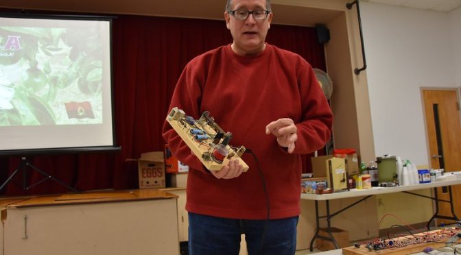
Charlie, AB1ZN Showing A Vintage Rig
Project night helped served to snap me back to reality. There I saw people work for months on projects, and no doubt encounters obstacles and challenges along the way, and they happily discussed who they went to for help and even welcomed advice and Elmering from club members after the presentations were finished. It was clear they were not discouraged by the challenges they knew they would face, and the time being invested into their project. And honestly, it made me feel a little better to see that even the best of us get stumped and need to collaborate. In fact, that is expected.
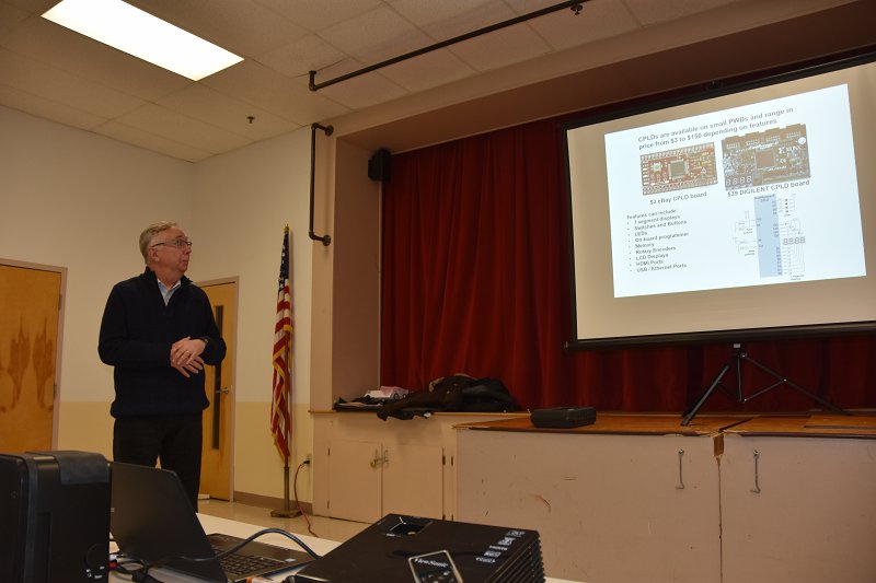
Hamilton, K1HMS Explains CPLD Technology
We have many experts in the club. Hamilton, (K1HMS), did a great job presenting a super-technical talk about CPLD’s.
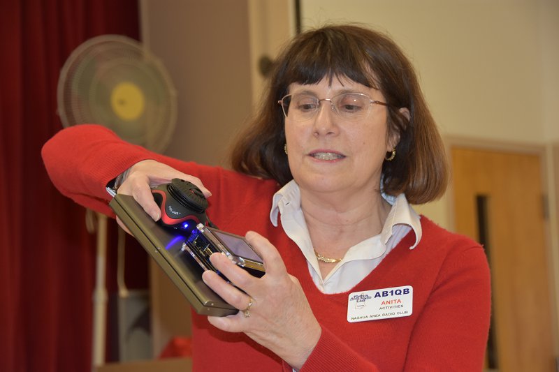
Anita, AB1QB Demonstrates her Raspberry Pi DX Alarm Clock
Anita, (AB1QB), had a really entertaining and pedagogical talk about software, DX spotting, Raspberry Pis, and annoying Fred (AB1OC) with DX alerts.
Mike, AB1YK Shows His Home-Build Transceiver
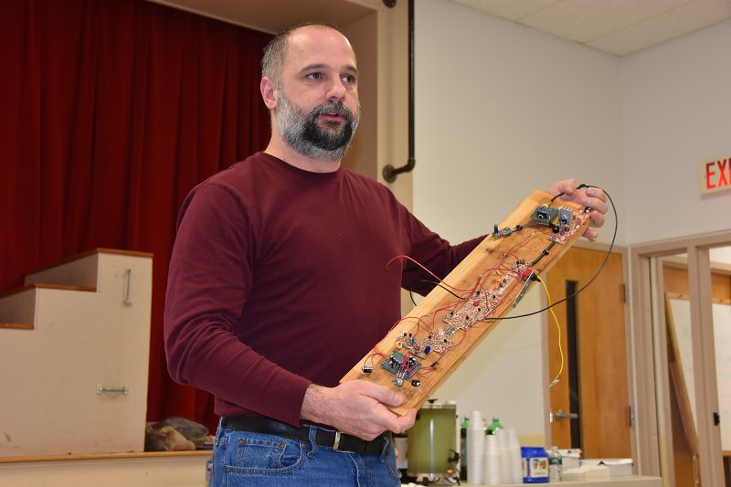
But one talk which really stood out in my mind was given by Mike (AB1YK) who said during his talk that he’s mainly a digital guy with a ton of Arduino experience. But, he was interested in diving into the analog world, and so his first foray into that world was to construct a QRP transceiver from scratch and teach himself what he needed.
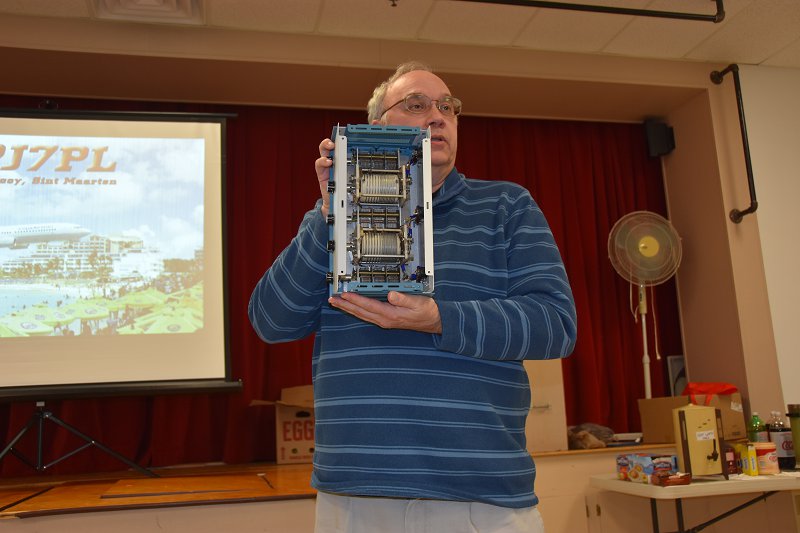
Jeff, WA1HCO Shows His Optimized Matching System
What last night was for me was inspirational. It gave me the peace of mind I needed to believe I can tackle subjects I really don’t know much about at all, and be somewhat successful at it. I won’t be a Hamilton, but I’ll know enough to make me dangerous, and that’s good enough for me.
Thank you, Nashua Area Radio Club members for opening my eyes, again. I look forward to crossing some of the projects I want to get busy on, off my list.
My “go to” tool when breadboarding is often an evaluation board with a Xilinx CPLD. A complex programmable logic device (CPLD) is a programmable logic device with complexity between that of PALs and FPGAs, and architectural features of both.
A CPLD is like a Digikey catalog on a chip. It includes simple logic devices like ANDs, NANDs, ORs, NORs, and XORs. There are Flip-Flops, FIFOs, MUXs, Counters, Compares, Latches, pull ups, pull downs, tri-state I/O, Schmitt triggers, and the list goes on and on. A small device has 64 user I/O ports and larger devices can have 100s of ports.
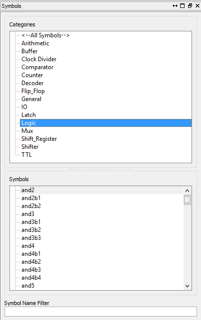
Figure-1 A wide range of devices is available.
Figure-1 is the pallet of available parts. The Category Logic is selected; the first 13 device showing are ANDs ranging from 2 to 5 inputs. An “and1b1″ is a simple AND with one standard input and 1 inverting input. There are also designs for RS-232/422, SPI, I2C etc on the web that are constructed from the pallet devices.
Once a symbol is placed on the schematic you can right click on the device and see its description and logic table. Most of the time the VHDL code is also available for editing if desired. Knowledge of VHDL or Verilog is not required to design at the schematic level. The schematic symbols are connected by placing a wire or bus between ports.
Ports can be configured into various I/O Standards. A “bank” can be configured for 5.0-volt logic and another bank can be 3.3V, 1.8V or 1.2V which is useful if you need “Glue Logic” between one standard and another.
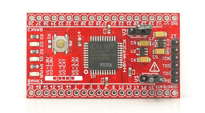
The best part is it is very easy to take advantage of this capability. There are numerous eval-boards priced from $3-$15 for a board like the one in Figure 2.
Figure-2 $10 CPLD evaluation board
At the $50 mark, you can get a board with LED lights/digits, buttons, switches, pots, etc.
At higher price points you can get USB, GB Ethernet, HD-LCDs and HMDI ports but they may be beyond schematic level designs and will require VHDL or Verilog skills.
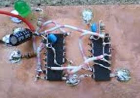
In contrast, there is the dead bug (Figure 2a) approach. The disadvantage to this approach is you must have the “bugs” on hand, the clock rate is limited to a few MHz due to wire length (CPLD clock speed can be > 125MHz), and “edits” are done with a soldering iron with the power off instead of a text editor with the circuit running.
Figure-2a Two dead bugs
The software tool to configure the CPLD is the Xilinx ISE WebPack which is a free download and a programming dongle that can range from $15 and up. Many boards include the programmer on the board eliminating the need for a dongle, all that is needed is a USB cable to the PC.
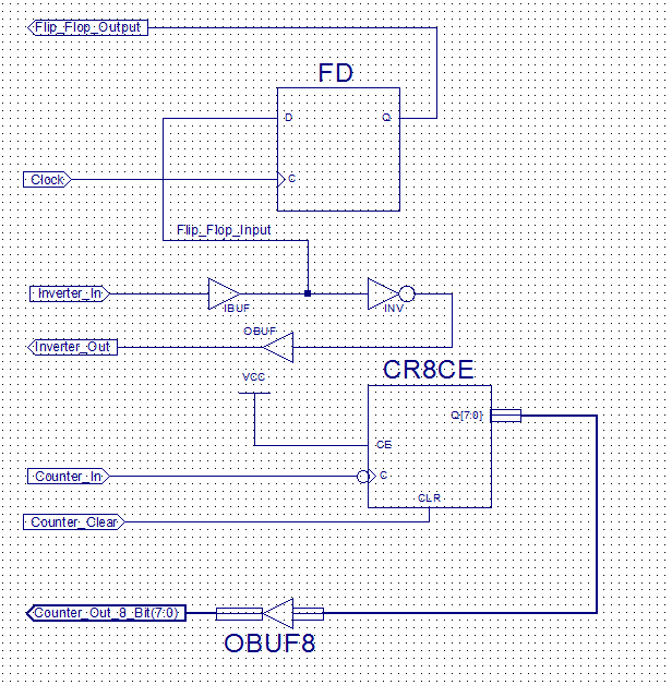
I have designed a small device in Figure-3 as an example. There are 3 distinct circuits. I have included an inverter for those times you have a signal that needs to be inverted, an 8 bit counter with a parallel output, and a Flip-Flop that shares the input with the inverter circuit.
Figure-3 Design ready to download onto a CPLD
The example shows an Inverter/Flip-Flop circuit and a counter circuit. They are independent of each other. The ability to have a large number of independent parallel circuits gives CPLD/FPGA an advantage over microprocessors in certain applications, especially DSP circuits.
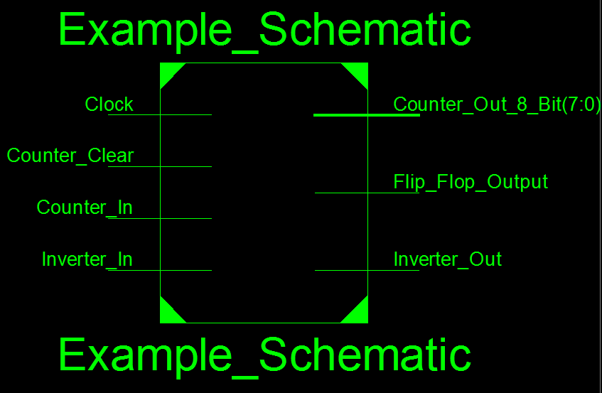
The Xilinx ISE tool will produce a block diagram (Figure-4) of the circuit.
Figure-4 Top Level Block Diagram
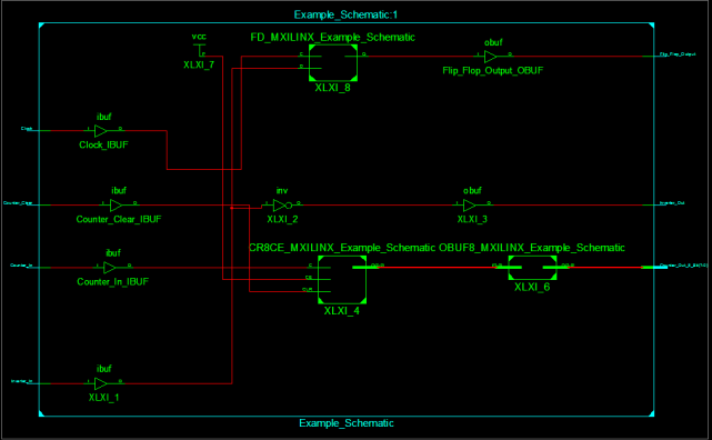
By clicking on the block diagram you can open the detailed circuit (Figure-5), further, the complex elements within the circuit can be expanded.
Figure-5 Detail Schematic produced from synthesized CPLD design
These are not a “redraw” of the original schematic. They represent the final design after the schematic was translated into HDL by ISE and a circuit design synthesized from the HDL code. This process is transparent to the user. This capability is very useful when designing in HDL. It allows you to discover errors in the code quickly. It is easier for many hardware designers to “debug” the firmware code by following wires on a schematic.
A CPLD board can be very useful in the Ham Shack when positive control is needed. In situations with multiple antenna switches, band switches, and amplifier keyer lines where control logic is important a CPLD design is a great approach. Once the required logic and lockouts are determined the logic design can be completed at the schematic level and the CPLD configured.
The CPLD uses Combinational Logic, it is completely deterministic. Even with a lot of care, a microprocessor has the potential to fall into a disallowed state that could potentially damage equipment. By using hardwired logic this becomes nearly impossible without an actual hardware failure.
If you find an error or change your station simply change the schematic and re-flash the CPLD. (The days of one-use fused link logic are behind us).
Xilinx ISE includes the capability to write a test bench where you describe the full range of inputs and it will display the corresponding output states and timing in Logic Analyzer style. The displayed data is based on actual physical device timing constraints and will allow you to trap switching glitches and logic errors.
While I have focused on CPLDs everything written above can be applied to FPGAs. The different is 100% transparent except the cost may be slightly higher for a small FPGA evaluation board. The first step up from a CPLD in the Xilinx line would be a Spartan device which has considerably most resources and higher performance. While schematic input is an easy place to start ISE is a widely used tool for both VHDL and Verilog HDL coding. It is hoped you would at least dabble in HDL once you have a board.
I have described getting started with CPLDs as easy. I find it much easier than coding in C where just keeping the tool set happy with its countless libraries that must be on the correct path and 100 other ways to generate errors. I enjoy coding in VHDL, for me, it is easier to “think” in terms of wires and buses. With that said there are a few minor hills to get over to start using ISE to configure a CPLD/FPGA.
Here are the three largest issues:
ISE WebPack is four 2 GB files. An 8 GB total download of compressed .tar files.
The process of generating and downloading the free license can be a challenge, and then you get to install it.
Getting an inexpensive aftermarket programming dongle to be recognized by ISE and the PC can require patience.
Once the program is installed and working the rest of the issues are nits. As a hardware designer, I consider them nits.
You can only attach one wire to a port pin if you want more than one it must be to a buffered pin.
The logic must be deterministic, in short, you cannot have two outputs tied together unless it is through a AND, OR or similar. Each connection must have a clear “true or false” state.
The ports you defined in the schematic must be routed to a pin on the CPLD. This is accomplished with a .ucf or User Constraint File. The constraint file format looks like this: NET “name” LOC = “P(pin number)”; That is it.
The following is part of the Constraint file for the schematic shown in Figure 3 and is compatible with the eval-board shown in Figure-2.
# This is an example of a constraint file
NET "Flip_Flop_Output"
LOC = "P5";
NET "Clock"
LOC = "P30";
NET "Inverter_In"
LOC = "P7";
#NET "P7"
LOC = "P1";
'#' indicates the line is commented out and is ignored
Most boards are supplied with a constraint file so you know which pins go to the switches and LEDs, and which ones you can use. If their names are P1, P2, P3 in the constraint file and you have named your ports Clock, Clear, and Count you will hang up on an error. The same is true if you do not use ports P7-P64 in the design and leave them un-commented in the constraint file. If it is in the design it must be in the constraint file, and vice-versa.
There is a short list of special Key words to include CLK, CLR, and NET. These and other Key words must be avoided until you get past the basics and understand their use.
ISE does a good job of providing a Web link for errors in ISE. The linked page will tell you the problem, likely cause, and the solution.
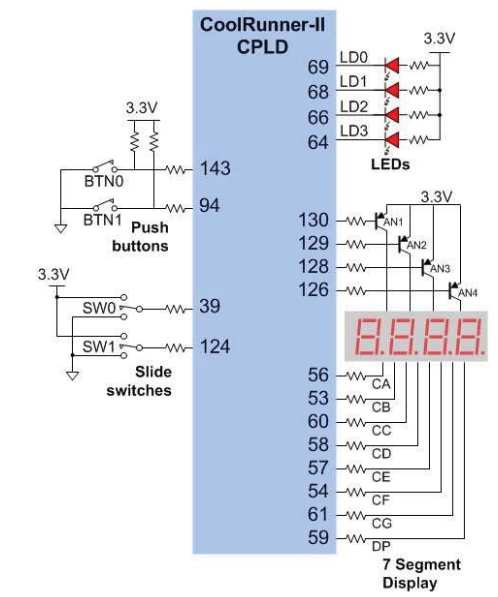
Here is a schematic of a 4 digit display, it still has 44 user pins available.
Figure-6 CPLD used to drive a 4 Digit Display
If nothing else ISE is a great way to draw schematics.
If you are interested in adding CPLDs and FPGAs to your tool kit I would be more than glad to get you set up and give you a short tutorial.
February 14, 2017, now represents two important days: Valentine’s and Nashua ARC’s Feb Tech Night! Nothing else says love like telling that special someone — you want to solder some electronics 🙂
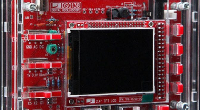
Back by popular demand (and good reviews from others) is our kit building night. Everyone had a blast on Election Night building the Pixie kits, and on V-day, we are going to work on a DIY oscilloscope known as the DSO138. (It is mere coincidence FYI that our kit building nights have fallen on holidays, of sorts).
The nice thing about this kit, of course, is being able to visualize some of the basic waveforms used in electronics. The kit does come with a square-wave test signal, but we will also have a signal generator present to visualize more complicated waveform.
Building this kit is an excellent opportunity to hone those soldering skills, brush up on electronics theory, and add another fun toy to your growing (or perhaps overflowing) collection. The price point is definitely fair for an oscilloscope and may help you figure out if you’ll want a more sophisticated one down the road.
We had about 15 people last time, so I think this time, it’d be great to expand that number to 20 (or more)! Buy a kit here, and join us in February! Looking forward to seeing you.