Tag Archives: HF

Spectral Purity of a QRP Transmitter Driver Amplifier

Introduction

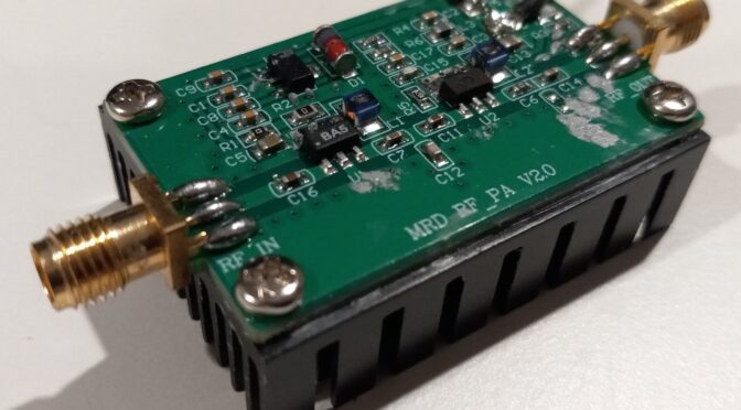
Some months ago, we reported on a commercially available, off-the-shelf 3W MMIC amplifier [1] to be used as part of a transmitter driver with receive bypass [2]. It was our intent to use as many COTS components as possible to simplify and shorten the construction timeline for a 10-band QRP SSB transceiver. An inexpensive amplifier that is widely available through AliExpress [3] is advertised to work from 2 to 700 MHz, which is more than adequate for our requirements (Figure 1. The gain of this amplifier was 45 dB.

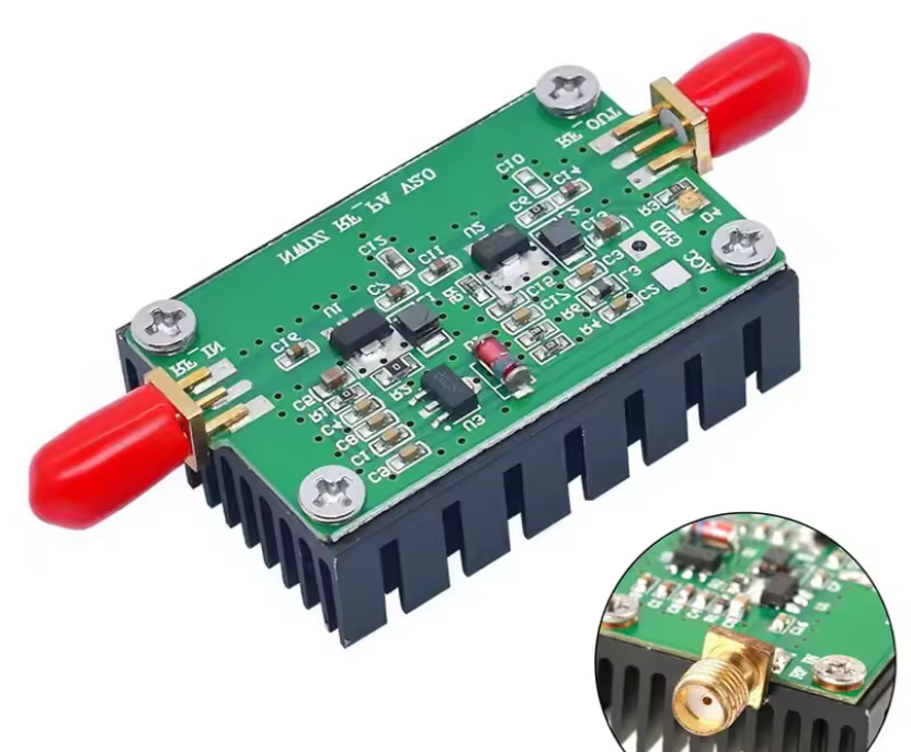
Figure 1. Wideband 3W Shortwave Amplifier. This wideband shortwave amplifier is advertised as being capable of 3W output power. Our plan is to drive it to 1W so that our 10 dB gain power amplifier can be driven to 10W. The 3W MMIC amplifier works from 2 to 700 MHz, which is more than adequate for high-frequency use. The measured gain of the amplifier is 45 dB. Power dissipation is greatly improved by the application of diamond heatsink compound between the circuit board and the heatsink. The amplifier is operated at +9 VDC to reduce its thermal dissipation. Please click on the Figure to open it in a new window.

Since our last report, some changes have been made to the original circuit to reduce its gain, increase its stability, improve its spectral purity, and enhance its receive isolation. The 3W MMIC amplifier is of single-ended construction. Consequently, there is no cancellation of even (or odd) harmonics of the signal being amplified, and it turns out that when operated at +9 VDC, or even +13.8 VDC, the MMIC amplifier is quite nonlinear.

This article discusses all of the circuit improvements. In particular, the spectral purity of the transmitter driver amplifier is demonstrated. Use of the single-ended amplifier requires the addition of another low-pass filter bank [4] between the driver amplifier circuit and the transmitter, in addition to the one that is provided at the transmitter output.

Low Pass Filter Bank

Thanks to Hans Summers, G0UPL, at QRP Labs [5] for providing bare boards so that my original filter bank, consisting of 10 low-pass filters, Figure 2, that employed the Ed Wetherhold (SK), W3NQN, design [6] could be built and tested.

As we will soon demonstrate, an additional low-pass filter bank results in greatly improved spectral purity. Since an additional low-pass filter bank had not yet been built, we have employed the transmitter low-pass filter bank, as required, for measurements in this paper.

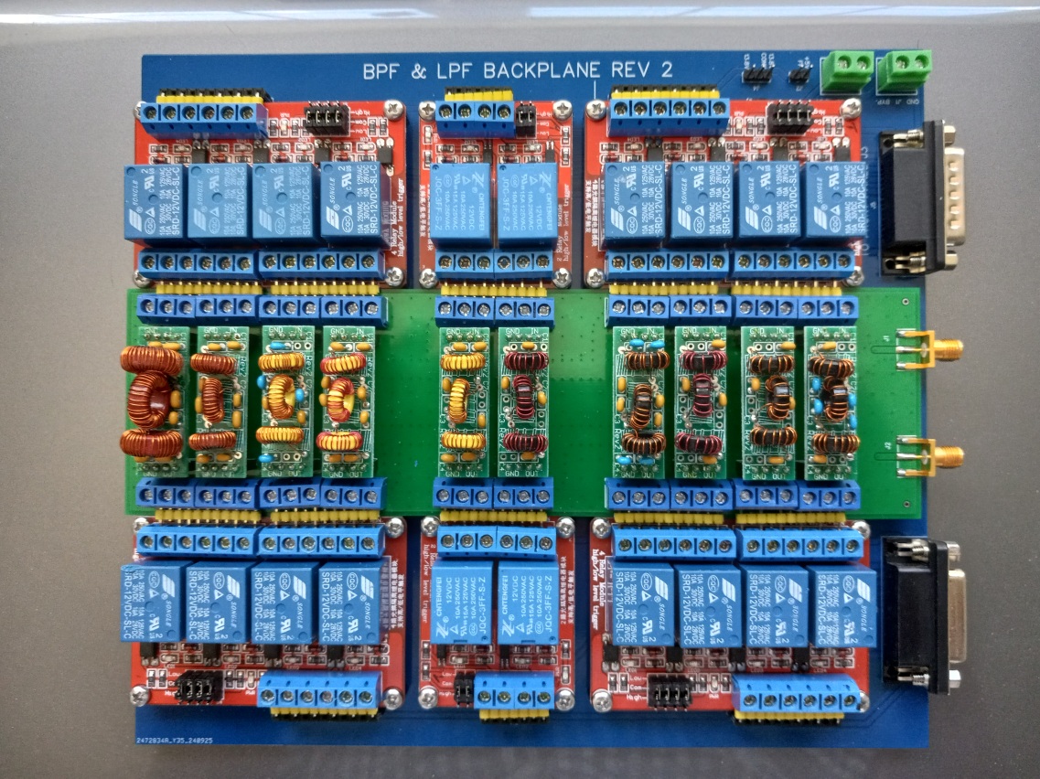
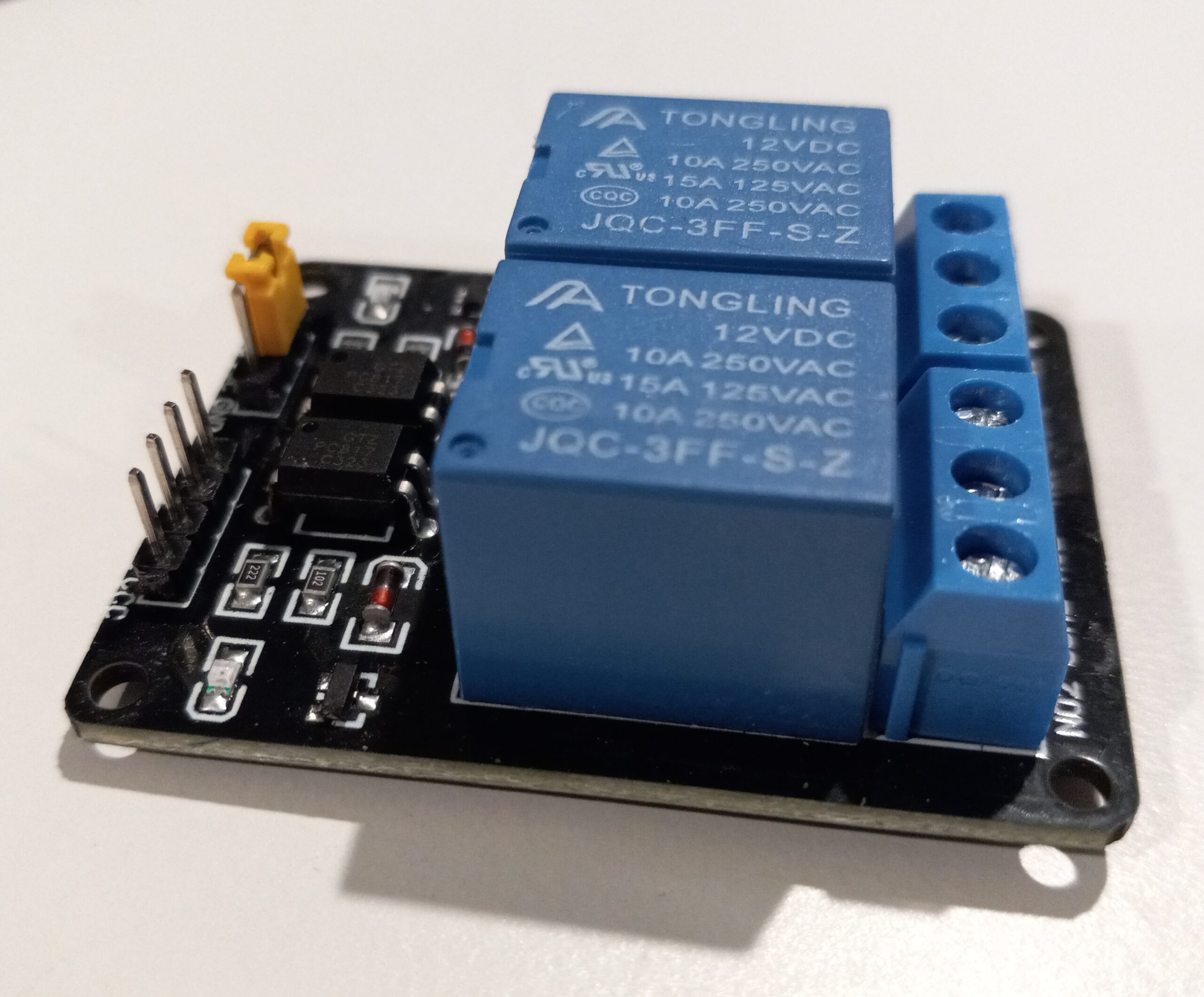
Figure 2. Ten-Band Low Pass Filter Bank on Its Interconnect Backplane. The 40m low-pass filter that was used to process the 7.1 MHz signal is located four filters from the left. All of the filters employ the Ed Wetherhold (SK), W3NQN, design. The bare boards for these filters were obtained from Hans Summers, G0UPL, at QRP Labs. Readily available Arduino relay boards were used throughout. Since these are power relays, the relay contacts are DC-wetted through bias-T’s, not shown, to reduce the contact resistance. The QRP Labs filters employ a single DPDT relay per filter band, whereas my filters employ two separate SPDT relays per band. Please click on the Figure to open it in a new window.

Revised Transmitter Driver With Receive Bypass Schematic
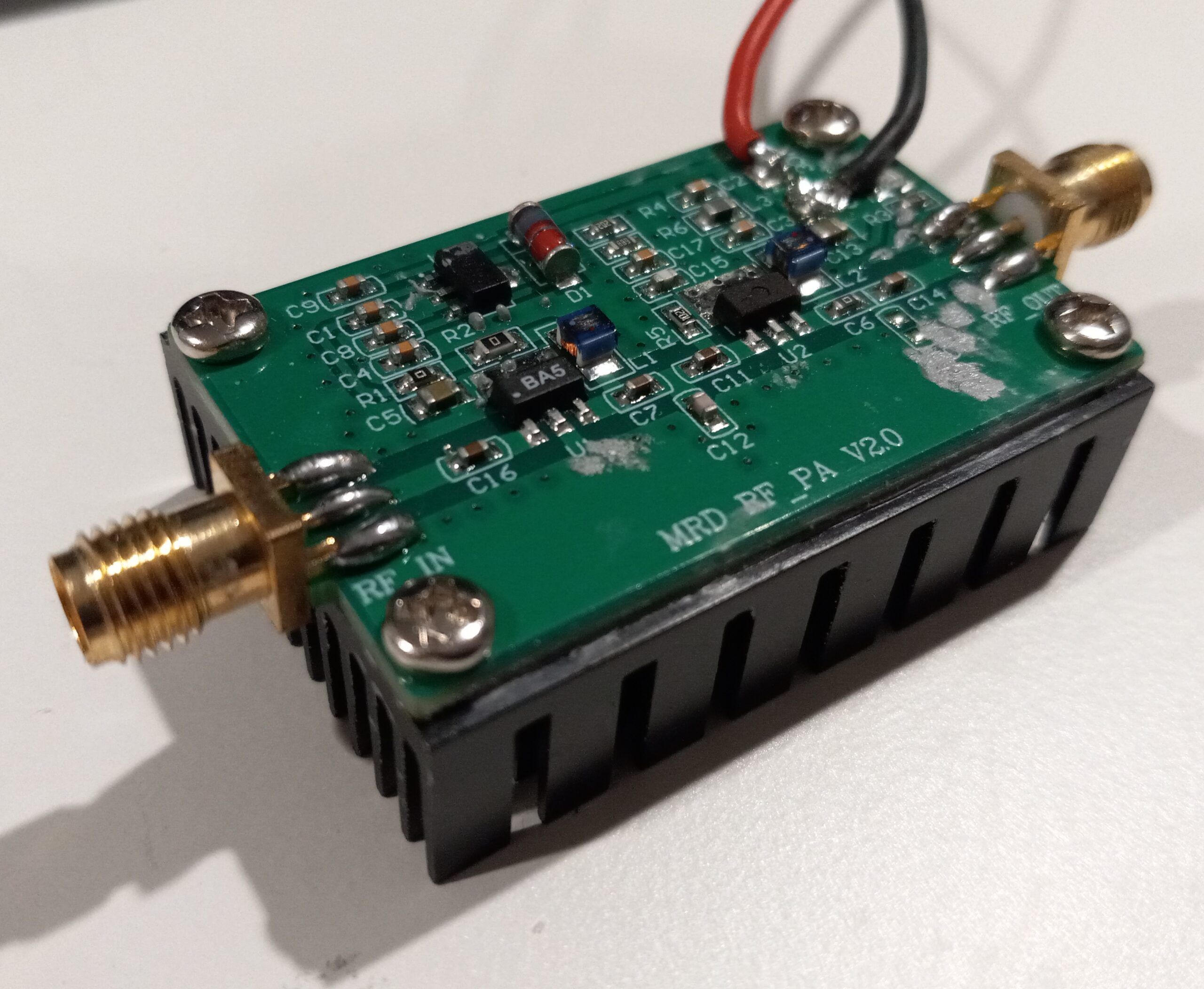
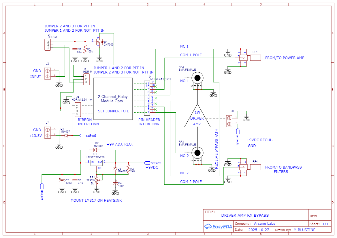
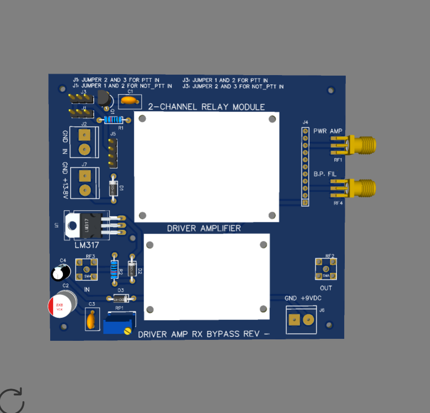
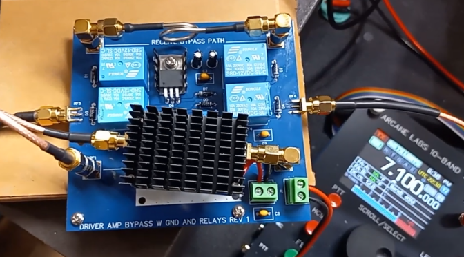
A revised schematic diagram is shown in Figure 3. Changes to the original design [7] include the removal of relay optical isolation for push-to-talk with the deletion of its attendant FET driver, and the addition of relay grounding for the receive bypass path during transmit. An additional relay pair was added to perform the grounding function. A 3 dB attenuator was added to the driver amplifier input to improve the amplifier stability and to reduce its gain. A photo of the completed design with the 3 dB coaxial attenuator installed is shown in Figure 4. If there is sufficient isolation, the 3 dB attenuator will be added to the back of the circuit card. The revised design uses a separate power management circuit board to supply +13.8 VDC to the +9 VDC onboard voltage regulator during transmit. This greatly simplifies the circuit board.

Figure 3. Revised Driver Schematic Diagram. The schematic has been simplified when compared to the previous iteration. The logic input has been removed so that the module may be keyed by the power management module during transmit. The receive bypass path is grounded at both ends during transmit. Power is supplied to the driver amplifier by an LM317 adjustable voltage regulator that receives power from the power management module during transmit. Please click on the Figure to open it in a new window.

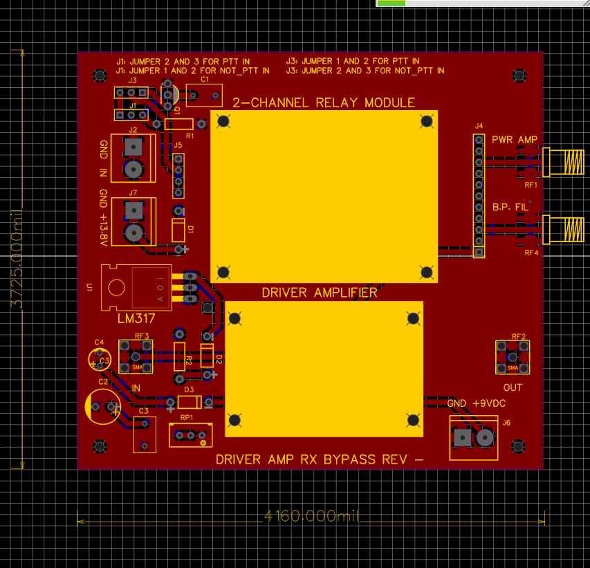
Figure 4. The Completed Driver Amplifier Board As Revised. The black driver amplifier heatsink is visible. The lower relay pair provides the transmit/receive function. The upper relay pair grounds each end of the semi-rigid coax receive path during transmit. The LM317 adjustable regulator regulates +13.8 VDC from the power management module down to +9 VDC for use by the driver amplifier. This reduces the amplifier power dissipation. Please click on the Figure to open it in a new window.

The measured spectrum of the amplified 7.1 MHz signal without low-pass filtering is shown in Figure 5. The amplifier has been driven to 1W. Since the amplifier is single-ended, the even harmonics have not been suppressed, and the 2nd harmonic is barely 10 dB below the carrier. It is evident that this MMIC amplifier is nonlinear.

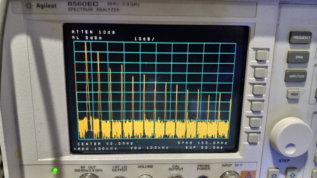
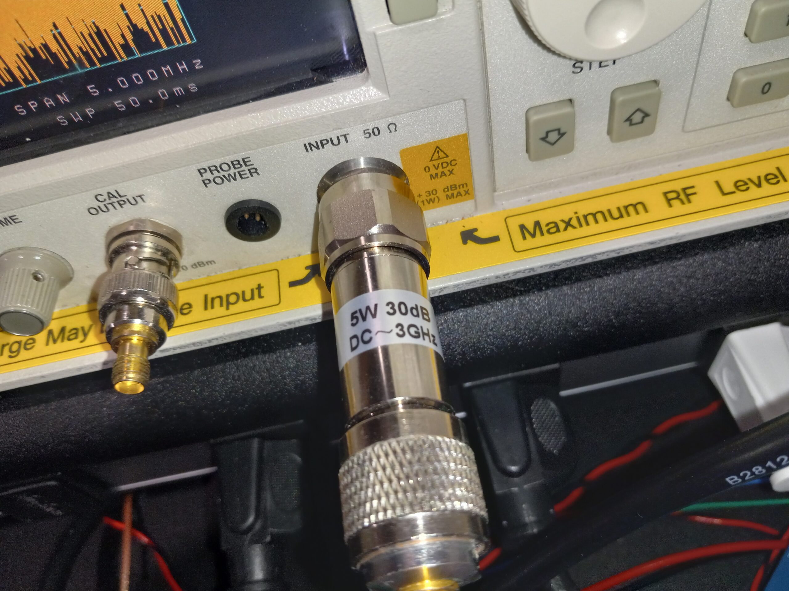
Figure 5. Spectral Purity of a 7.1 MHz Signal Prior to Low Pass Filtering. Even and odd harmonics are visible because the driver is single-ended, not push-pull. A push-pull amplifier would provide some attenuation of the even harmonics but not the odd harmonics. The spectrum analyzer display shows the 7.1 MHz carrier at 0 dBm. Since the spectrum analyzer input is padded by 30 dB, 0 dBm corresponds to 1W. The second harmonic is barely -10 dBc for this drive level. Please click on the Figure to open it in a new window.

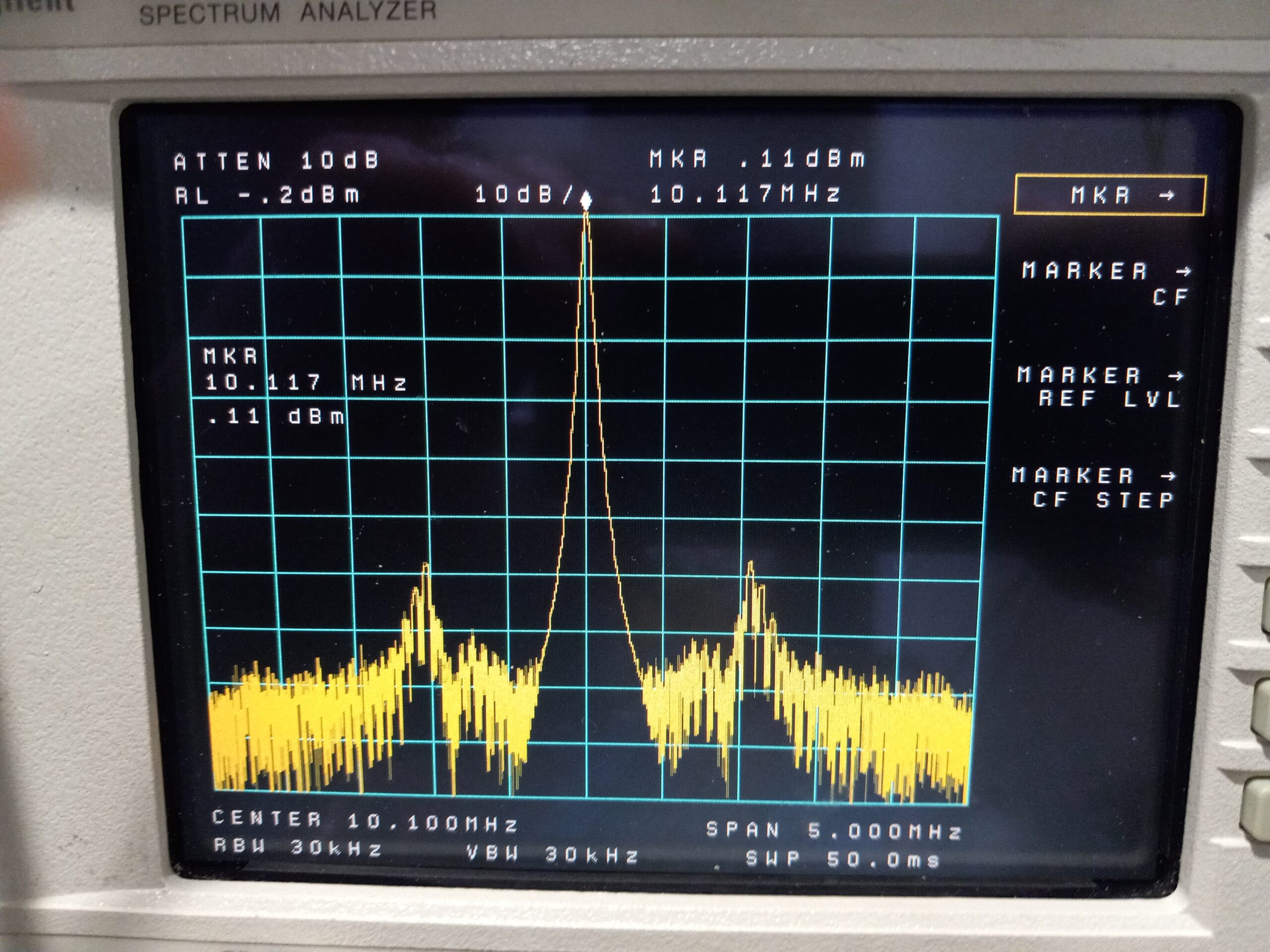
The measured spectrum of the amplified 7.1 MHz signal with low-pass filtering is shown in Figure 6. The amplifier drive level was left unchanged from the previous measurement. With the low-pass filter applied to the signal, both the even and odd harmonics have been suppressed by nearly 60 dB.

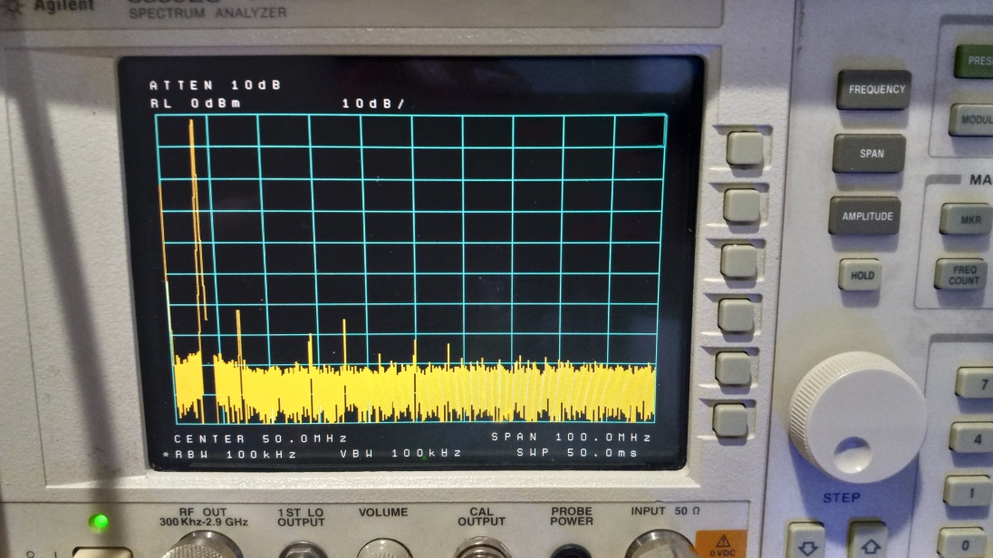
Figure 6. Spectral Purity of a 7.1 MHz Signal After Low Pass Filtering. The even and odd harmonic content of the 7.1 MHz signal has been suppressed by nearly 60 dB. The implication is that the W3NQN 40m low-pass filter is doing a great job of attenuating the 2nd harmonic and higher-order products. About 1 dB of signal attenuation is observed after passing it through the low-pass filter, as one might expect. As in the previous figure, 0 dBm corresponds to 1W due to the presence of a 30 dB pad at the spectrum analyzer input. Please click on the Figure to open it in a new window.

Summary

We have described revisions to the original circuit design that result in a much simpler driver amplifier that retains a receive bypass function. The revised circuit is keyed from the power management module on transmit so that it does not have to be keyed directly from push-to-talk.

The spectral purity of the amplified signal before and after low-pass filtering has been demonstrated. Higher order harmonics are attenuated by nearly 60 dB by Ed Wetherhold, W3NQN, low-pass filters.

The low-pass filter bank that was used for spectral evaluation is at the transmitter output. Consequently, another low-pass filter kit has been ordered from QRP Labs that will cover 5 of the 10 bands. Another kit will be ordered at a later date to cover the remaining 5 bands. Since these low-pass filters come without an integral transistor interface for microprocessor I/O, one will have to be built.

A short YouTube video [8] of a test may be viewed at https://youtu.be/nTQk9CR1W9w

References

[1] 2 MHz-700 MHZ 3W HF VHF UHF FM Transmitter RF Power Amplifier For Radio https://www.aliexpress.us/item/3256807249993037.html?spm=a2g0o.order_list.order_list_main.25.1adb1802la12vX&gatewayAdapt=glo2usa

[2] Blustine, Martin, RF Driver Amplifier With Receive Bypass, N1FD, Nov. 1, 2025. https://www.n1fd.org/2025/11/01/rf-driver-amplifier/

[3] AliExpress, op. cit.

[4] QRP Labs, Ultimate Relay-Switched LPF Kit, https://qrp-labs.com/ultimatelpf.html

[5] QRP Labs, Low Pass Filter Kit, https://qrp-labs.com/lpfkit.html

[6] Wetherhold, Ed, W3NQN, Second-Harmonic Optimized Low-Pass Filters, QST, Feb. 1999, pp. 44 – 46.

https://www.arrl.org/files/file/Technology/tis/info/pdf/9902044.pdf

[7] Blustine, Martin, op. cit.

[8] YouTube Test Video, https://youtu.be/nTQk9CR1W9w

Disclaimers

This circuit design is provided for informational and educational purposes only and is supplied “as is” and without warranties of any kind, express, implied, or statutory. No representations or warranties are made regarding the accuracy, adequacy, completeness, legality, reliability, or usefulness of this information, either in isolation or in the aggregate. This circuit design may contain links to or information based on external sources or third-party content. Endorsement and responsibility for the accuracy or reliability of such third-party information or for the content of any linked websites are not taken.

N1FD Winter Field Day 2026

The Nashua Area Radio Society (N1FD) successfully completed Winter Field Day 2026, operating on January 24–25 under some of the harshest winter conditions we’ve experienced in recent years. Bitter cold persisted throughout the weekend, followed by a snowstorm on Sunday afternoon, yet the club achieved all planned multipliers and delivered a strong overall result.

N1FD operated as Class 2H, with all stations located indoors at the QTH of Fred Kemmerer, AB1OC, and Anita Kemmerer, AB1QB. Antennas were deployed outdoors, allowing operators to remain warm, safe, and focused while fully meeting the operating and technical challenges of Winter Field Day.

N1FD Team Putting Up the Wire Antennas in the Prep Session on 12/20

Preparation Made the Difference

Winter Field Day success was the result of careful planning and coordination in the weeks leading up to the event. The club focused on targeting specific band and mode multipliers, ensuring coverage across HF, VHF, and UHF, coordinating operator schedules and operating strategies, and verifying station readiness and antenna performance.

That preparation paid off, allowing N1FD to methodically work bands and modes and complete every planned multiplier without last-minute pressure.

QSO and Band Results

During the weekend, N1FD logged:

BandModeQSOsPts
160 mCW55110
80 mLSB2020
40 mLSB8181
20 mPSK3112
20 mUSB445445
15 mUSB337337
10 mUSB8181
6 mUSB33
2 mFM33
1.2 mFM33
70 cmFM33
33 cmFM33
23 cmFM33
TotalAll10381094

1,038 total QSOs
1,094 total QSO points
28 total multipliers
Based on these results, N1FD’s estimated final score was:

1,094 QSO points × 28 multipliers = 31,726 points

The strongest activity came from 20 meters (USB) and 15 meters (USB), with solid participation across 40 meters, 80 meters (CW), digital modes, and successful contacts on VHF and UHF, all of which were critical to completing the multiplier plan.

Multipliers Achieved

A major objective for Winter Field Day 2026 was to intentionally pursue as many multipliers as possible through planning and disciplined operating. N1FD successfully completed every multiplier we set out to achieve, resulting in a total multiplier of 29X, including the 1X multiplier added for participation.

The following multipliers were earned during the event.

N1FD Multipliers Achieved

Completing the full multiplier set was a direct result of advance planning, operator coordination, and flexibility throughout the weekend.

Fred AB1OC Working on Multipliers while Anthony KC1DXL Operates SSB

Operators on the Air

The following members operated under the N1FD callsign during Winter Field Day:

Operators rotated across bands and modes to keep stations active and productive throughout the event.

HTs Covering 2m - 23cm
HTs Covering 2m – 23cm

VHF Rover Participation

In addition to the fixed indoor stations, three N1FD members participated as VHF Rovers, helping us to achieve the 12-band multiplier.

Their rover operations added an important mobile element to N1FD’s Winter Field Day effort.

Special Thanks

Special thanks go to Joe Luszcz, AC1LN, and Brian Quick, W1XMM, who installed the wire antennas on Friday, January 23rd, working outdoors in very cold weather to ensure the stations were fully operational before the event began.

Additional recognition goes to Fred Kemmerer, AB1OC, who spent many long hours preparing the station, testing equipment, and resolving technical details ahead of Winter Field Day. His dedication was critical to the smooth operation and success of the weekend.

We would also like to thank Brian Quick, W1XMM, for his leadership in planning and coordinating Winter Field Day 2026 in his role as Field Day Chairman. His organization and preparation were instrumental in helping the club meet its operating and multiplier goals.

Special thanks to Dave Cherkus, N1AI, for operating 160-meter CW, helping N1FD make effective use of the low bands during challenging winter conditions.

Thank you to Dave Berardinelli, K1BER, for leading and coordinating the VHF Rover effort, which played an important role in expanding our band coverage and multiplier success.

Finally, thank you to all of the operators who participated throughout the weekend. Your time, flexibility, and teamwork made this Winter Field Day a success.

A Successful Winter Operation

Winter Field Day 2026 once again demonstrated what N1FD does best: strong planning, teamwork, and adaptability, even under challenging winter conditions. Operating indoors allowed the club to stay safe and effective while still delivering excellent on-air results.

Thank you to everyone who planned, set up, operated, and supported this effort. We look forward to building on this success for future Field Days and operating events.

RF Driver Amplifier Circuit With Receive Bypass

This article discusses how a 3W commercial off-the-shelf (COTS) amplifier [1] may be used to drive a COTS 30W power amplifier [2] for use in a QRP transceiver transmitter. When homebrewing, it can be challenging to determine when to design and build something from scratch or when to assemble it from COTS parts. Several low-power amplifiers were considered for use as driver amplifiers, and the one selected is capable of a 1W (+30 dBm) output with only 0.032 mW (-15 dBm) input, resulting in a 45 dB gain at 10.12 MHz. This amplifier works over the entire HF spectrum. The 30W power amplifier was advertised for use as a linear amplifier that follows a low-power transceiver. It is provided with a receive bypass relay circuit so that the received signal will pass through the linear amplifier unimpeded. The 3W amplifier, however, does not have a receive bypass circuit. To use it in this application, a receive bypass path must be provided. That is the subject of this article.

Component Parts

The 3W amplifier selected for this application is shown in Figure 1. It consists of two Monolithic Microwave Integrated Circuits (MMICs) cascaded to produce the specified gain and power output. It was acquired from a seller on AliExpress [3] for less than $15. Upon arrival, the circuit board was removed from its heat sink. That is when it was discovered that no thermally conductive paste of any kind was applied to the interface. The ground tabs on the MMIC amplifiers were designed to dissipate heat. However, the only conduction path is through the via holes in the circuit board in proximity to the ground tabs. This is an ineffective conduction path to the ground plane on the rear side of the circuit board.

RF Driver Amplifier

Figure 1. A Commercial-Off-the-Shelf MMIC Driver Amplifier. This is a commercially available MMIC amplifier with an advertised output power of 3W. When operated with 12 to 15 VDC, the amplifier overheats. There was better luck once a layer of diamond thermal compound had been spread between the circuit board and the heatsink. Once reassembled onto its heat sink, the amplifier ran lukewarm at an operating voltage of +9 VDC with a power output of 1W (+30 dBm) when driven with 0.032 mW (-15 dBm). If the photo is studied closely, the grey thermal compound may be seen finding its way to the top of the PCB through the PCB via holes. Please click on the image to open in a new screen.

Once diamond thermal compound {4] had been applied to the back of the circuit board, the thermal paste began to fill the via holes thereby increasing the area of the conduction paths to the rear ground plane and to the heat sink beneath.

Next, operation was attempted at +13.8 VDC. While not hot enough to boil water, the heatsink became uncomfortably warm with the module dissipating more than 6W. Clearly, something didn’t seem quite right. These modules were specified for operation between +12 VDC and +15 VDC for the stated output power. The reliability of operation at this temperature was questionable.

If the heat sink area and volume is not increased, the simplest remedy is to reduce the operating voltage. Operation at +9 VDC was investigated with very good results. The RF power output of the module at 10.12 MHz is shown in Figure 2. The modulation sidebands are due to the bench switching power supply used. An output power of 1W (+30.11 dBm) was achieved for  0.032 mW (-15 dBm) input power, and the power dissipation dropped to 3W. One watt is more than enough power to drive the power amplifier to 10W (+40 dBm). When cooled by the fan in the transmitter, the MMIC driver amplifier will operate reliably.

Figure 2A

Figure 2B

Figure 2. Output Power of the 3W MMIC Driver Amplifier. At A, the spectrum analyzer photo is of the amplifier output power at 10.12 MHz. The modulation sidebands that originate with the switching power supply are visible. An output power of +0.11 dBm is observed. At B, since a 30 dB attenuator protects the spectrum analyzer input, the actual power achieved is 1W (+30.11 dBm) for -15 dBm input power. The gain at +9 VDC operating voltage is 45 dB. This is 10 dB higher than the specified gain, at least at 10.12 MHz. Please click on each image to open in new screens.

The 2-channel relay selected for this application is shown in Figure 3. These are commonly referred to as Arduino relays. Typically, they are operated from the TTL outputs of an Arduino after inversion. The relays may be operated with positive logic or negative logic by moving a small jumper. The relay inputs are optically isolated which greatly simplifies their use.

Figure 3. A 2-Channel Arduino Relay. These relays are optically coupled and can be controlled with positive and negative logic by moving the tan jumper that is visible in the photo. This module consists of two discrete, individually controllable single pole double throw (SPDT) relays. Please click on the image to open in a new screen.

Voltage regulation is provided by the LM317 adjustable voltage regulator [5]. The ripple output of the device is not of concern because it is being operated from a bench power supply. The voltage adjustment potentiometer has been bypassed; nonetheless, since the ripple voltage tends to increase with increasing adjust resistance.

A 2N7000 MOSFET is selectable at the logic input to the relay pair. If selected, it serves two purposes; a high impedance logic input for CMOS as well as a method for logic signal inversion, if desired, at the relay input.

Circuit Design

The circuit was designed on EasyEDA [6], a free, easy-to-use online design software package. As is usually the case, the Gerber files were transmitted to JLCPCB [7], a printed circuit fabrication house in Hong Kong. Turnaround time is typically 5 to 10 days depending upon the complexity of the circuit.

The circuit schematic diagram is shown in Figure 4. All of the key components of the previous section are shown on the schematic. Note that the receive path is through the normally closed contacts of the relays. Thus, no relay coil current is required during receive.

RF Driver Amplifier

Figure 4. Driver Amplifier Receive Bypass Schematic Diagram. The module has been designed around readily available COTS component parts. All parts are of the through-hole variety since there is little area to be gained through the use of SMT because the amplifier and relay are so large. Please click on the image to open in a new screen.

The jumpers for logic high input and logic low input operation are shown next to J1 and J3. Some of the connections to the relay are made with pin headers and Dupont ribbon wires. Power connections to the driver amplifier are made by connecting wires to screw terminal, J8.

Through-hole components are used in construction. Surface mount (SMT) parts would not reduce the area of the circuit board by much because the 2-channel relay board and 3W driver amplifier are relatively large, and the driver amplifier connects to the circuit board with right angle SMA adapters.

Two SMA connectors provide circuit I/O.  SMA connecter, RF4, provides the interface to the transceiver bandpass filters while SMA connector, RF1, provides the interface to the power amp.

The relay coil is operated with supply +13.8 VDC while the driver amplifier is operated with regulated +9 VDC.

The circuit board layout is shown in Figure 5. Places for the 2-channel relay with mounting holes and the driver amplifier with mounting holes are provided. The driver amplifier will be connected to the PCB with right angle SMA-male to SMA-male adapters.

Figure 5. Driver Amplifier Receive Bypass Circuit Board Layout. This is the silkscreen view of the assembly. The dimensions of the board are visible in the photo. Please click on the image to open in a new screen.

A 3-D rendering of the design is provided in Figure 6. Please note that some of the components are missing because 3-D models were not provided for the entire online library.

Figure 6. A 3-D Rendering of the Driver Amplifier Receive Bypass Circuit Board Layout. This 3-D virtual reality image was generated by EasyEDA. Some of the components are missing because 3-D images of the parts were not found in the library. Please click on the image to open in a new screen.

Conclusions

A design has been described that may be useful in conjunction with just about any RF amplifier for use in ham radio transceivers. The amplifier receiver bypass described in this paper will permit bi-directional operation as is required in one direction on transmit and the opposite direction on receive.

References

[1] https://www.aliexpress.us/w/wholesale-3W-shortwave-amplifier.html?g=y&SearchText=3W+shortwave+amplifier&sortType=price_asc

[2] https://www.aliexpress.us/w/wholesale-30W-shortwave-amplifier.html?spm=a2g0o.productlist.search.0

[3] 3W shortwave amplifier. Op. cit.

[4] https://www.amazon.com/JunPus-JP-DX2-Diamond-Thermal-Grease/dp/B0D7ZB43CF/ref=sr_1_1?crid=2Y1JXHD9J9MJZ&dib=eyJ2IjoiMSJ9.4cYW0erokqTHc7fpr9sWpA.vo3kXvGYCUoitzHMexiezvzYV0lb71EJvz3U3OOC614&dib_tag=se&keywords=JP-DX2-JunPus&qid=1761789390&sprefix=jp-dx2-junpus+%2Caps%2C85&sr=8-1

[5] https://www.ti.com/lit/ds/symlink/lm317.pdf

[6] https://easyeda.com/

[7] https://jlcpcb.com/

Disclaimers

This circuit design is provided for informational and educational purposes only and is supplied “as is” and without warranties of any kind, express, implied, or statutory. No representations or warranties are made regarding the accuracy, adequacy, completeness, legality, reliability, or usefulness of this information, either in isolation or in the aggregate. This circuit design may contain links to or information based on external sources or third-party content. Endorsement and responsibility for the accuracy or reliability of such third-party information or for the content of any linked websites are not taken.

Radio Amateurs Developing Skills Worldwide