
Introduction
Some time has passed since the last article [1] was written about this homebrew 10-Band SSB transceiver and its many modules. This article will focus on the receiver portion of the transceiver and its level of integration to date.
The motivation for taking on a project of this magnitude came from following many avid homebrewers including, but not limited to, Rick Scott, N3FJZ; Wes Hayward, W7ZOI; Bob Kopski, K3NHI; Jason Milldrum, NT7S; Pete Juliano, N6QW; Charlie Morris, ZL2CTM; Alan Wolke, W2AEW; Ashhar Farhan, VU2ESE; Nick Wood, M0NTV; Don Huff, W6JL; and Hans Summers, G0UPL.
It has been a slog. For example, the Lowpass and Bandpass Filter Assemblies were completed 8 years ago while we were living in Florida. The Lowpass and Bandpass Filter Assembly Backplanes that interconnect the filter logic control and DC wiring to form complete filter modules were completed only 2 years ago. The delays in completion of this project have been due to a series of life events.
I would like to acknowledge the thousands of lines of code attributable to Rick Scott, N3FJZ, without whose mentoring and incessant encouragement this radio would not have reached this level of complexity or state of completion. If you haven’t visited his webpage [2] or his YouTube channel [3], I would highly recommend it.
While this radio contains some original design work, this single-conversion, analog radio design borrows, shamelessly, from any number of well-known, serious amateur radio homebrewers, including Rick. The names of these titans are cited throughout this article. Where possible, and to save time and money, commercial subassemblies were purchased for integration into larger assemblies. For example, the Wes Hayward, W7ZOI, and Bob Kopski, K3NHI, bidirectional termination insensitive amplifiers (TIAs) may be purchased from multiple sellers [4] [5] [6].
It was never intended for this radio to be fully integrated. It was intended to be a highly reconfigurable breadboard to be spread across the workbench. Consequently, no particular attention was paid to vertical interconnects for packaging. With some encouragement from N3FJZ, who was light-years ahead in his packaging concept, I began to rethink how I might package what I had already built.
As a result, there are several subminiature-D connectors that surround the assembly stackup. In the short term, these outcroppings may be mitigated by redesigning the interconnects with PCB-mounted right-angle subminiature-D connectors. Then, the wiring might hug the assembly more closely. This, at bare minimum, would be necessary if the Multifunction Audio Processor Module [7] is to be installed on top of the stackup.
Over the long term, the positions of several of the connectors would have to be moved into better alignment between layers of the stackup to support vertical interconnects.
All of the PCB design work, including the Control Panel escutcheon, was completed using EasyEDA [8], a free online graphics tool. All boards were fabricated in Hong Kong by JLCPCB [9].
Receiver Description
A receiver description is contained in the sections that follow. It is in no way comprehensive, but it provides enough detail to describe some of the receiver performance, hardware functions, and its features.
The entire transceiver architecture, borrowed from N3FJZ, is shown in Figure 1 [10]. The receiver portion of the design is a single-conversion superheterodyne. Although performance is vastly improved over that of a homodyne receiver that converts the RF signal directly to audio using a local oscillator tuned to the same frequency as the RF, a single conversion design suffers from the lack of Image Rejection unless mitigated in receiver design.
The receiver described in this article differs somewhat from the block diagram. First, power management is accomplished by switching power MOSFETs when push-to-talk is asserted. I attribute this design to N3FJZ. Second, an S-meter voltage may be derived from the audio signal amplitude as shown in Rick’s diagram or in an alternative IF to Baseband Converter with AGC Module, where it may be derived from the AGC voltage. Third, the bandpass and lowpass filter banks have been expanded to encompass 10 bands, as supported by the current software build. Fourth, a broadcast interference notch filter has been added to the receive bypass path for general coverage.
In addition to these features, a higher-power audio amplifier and automatic audio leveling are provided. These two features have been tested individually, but they have not been integrated into the receiver, as they reside on a much larger Multifunction Audio Processor Module [11] that also contains some additional transmit audio features.
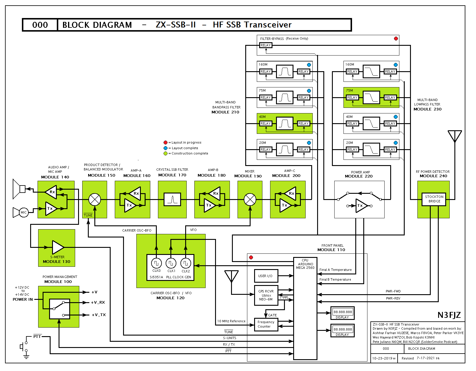 Figure 1. 10-Band Transceiver Block Diagram. This transceiver block diagram appears in N3FJZ’s ZX-SSB-II multiband homebrew SSB HF transceiver web pages. It is an earlier design that contains a receiver bypass path to bypass the lowpass and bandpass filters so that general coverage stations in the shortwave bands may be received. A Broadcast Interference (BCI) Notch Filter Module [12] (to be described later) has been added to this path to reduce strong, local AM broadcast stations by 70 dB. The same signal that asserts the receive bypass command for general coverage is used along with the push-to-talk command to inhibit the transmitter when the radio is tuned to general coverage bands [13]. Instead of relays, MOSFETs are used for Transmit/Receive Power Management. The current software build supports filter switching for 10 ham bands. Please click on the figure to open it in a new window.
Lowpass Filter Sources of Supply
The lowpass filters were built on circuit cards supplied by QRP Labs [14]. The component values are those appearing in the Ed Wetherhold, W3NQN, paper on the subject of Second-Harmonic-Optimized Low-Pass-Filters [15]. The highly stable NPO capacitors were purchased from Digikey [16] and Mouser [17], while the ferrite cores were purchased from Kits and Parts [18]. Enameled coil wire was sourced on Amazon [19].
Lowpass Filter Assembly
The lowpass filters used in the 10-band filter bank are of the Ed Wetherhold, W3NQN (SK), design [20]. They employ a series resonator that will greatly suppress the second harmonic of the transmitter signal. Upon receive, the lowpass filter functionality is more limited.
The Lowpass Filter Assemblies as they appeared 8 years ago are shown in Figure 2. They lack an interconnection backplane that serves to bring all of the logic connections to a single connector. The SMA connectors are launchers for the coplanar waveguide that resides on the back of the green PCB.
Arduino relays are used for filter switching. Since they are power relays, the contacts tend to oxidize if they are used for signal purposes. This oxidation may be mitigated by introducing a small, 20 mA current through the relay contacts with a bias-T (not shown) to “wet” the relay contacts.
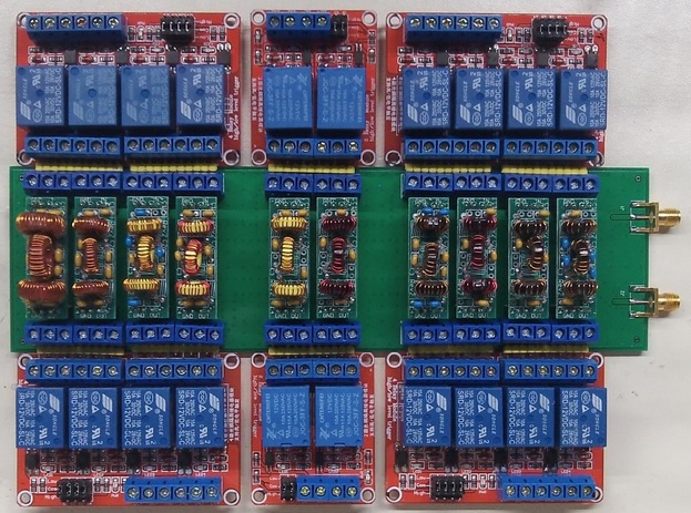 Figure 2. Lowpass Filter Assembly. It was lacking an interconnection backplane for DC power and logic connections. The SMA launchers are soldered to the end of a coplanar waveguide that resides on the bottom side of the green circuit card. Please click on the figure to open it in a new window.
Lowpass Filter Backplane
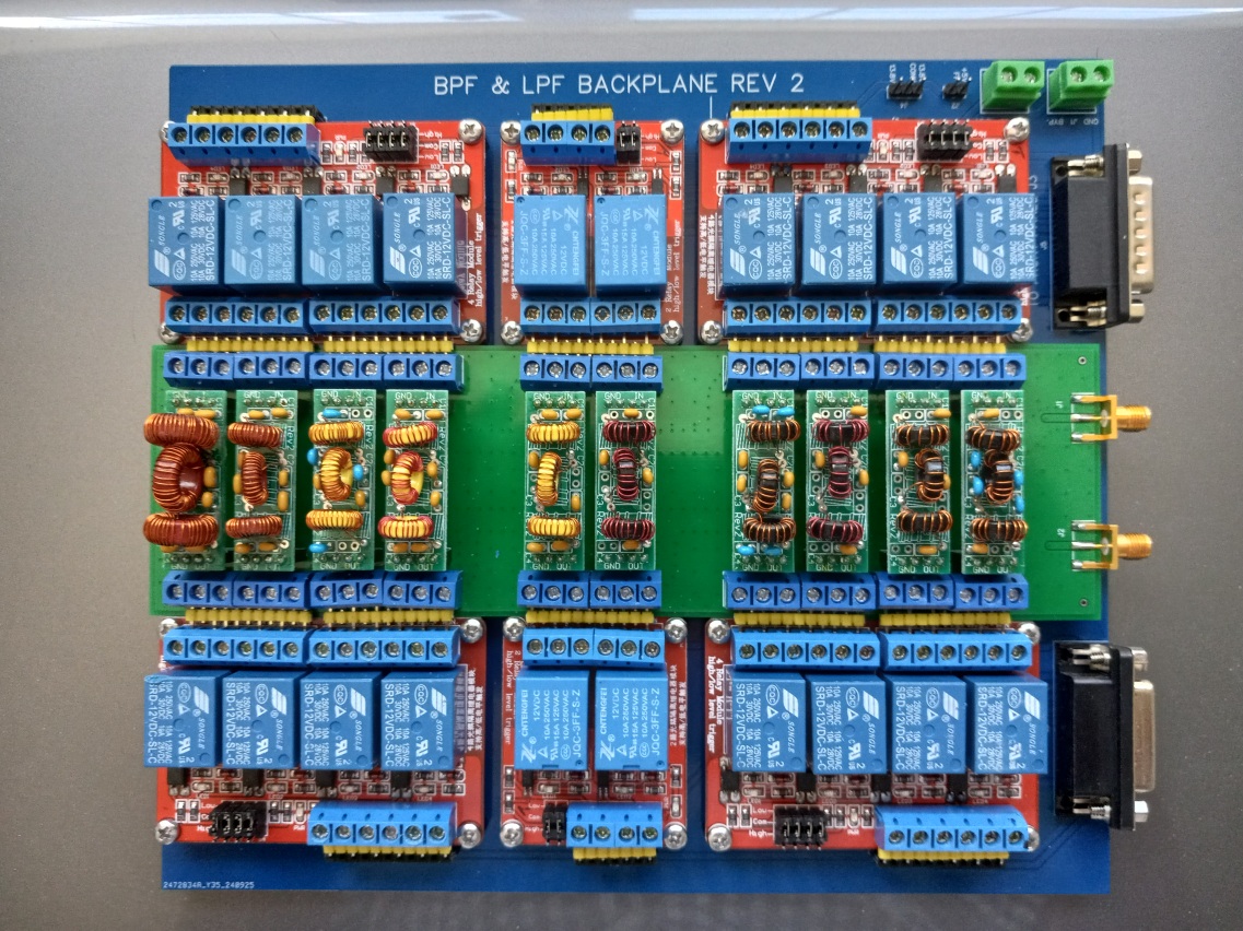
A means for connecting 10 lowpass filters to DC relay power and logic was not completed until 2024. The completed Lowpass Filter Backplane Assembly is shown in Figure 3. Provision is made for two subminiature-D connectors. Two are required because one of them (top right) receives its logic signals from the Arduino Front Panel, and it passes these same logic signals to the Bandpass Filter Backplane in the layer above from the subminiature-D connector at the lower right.
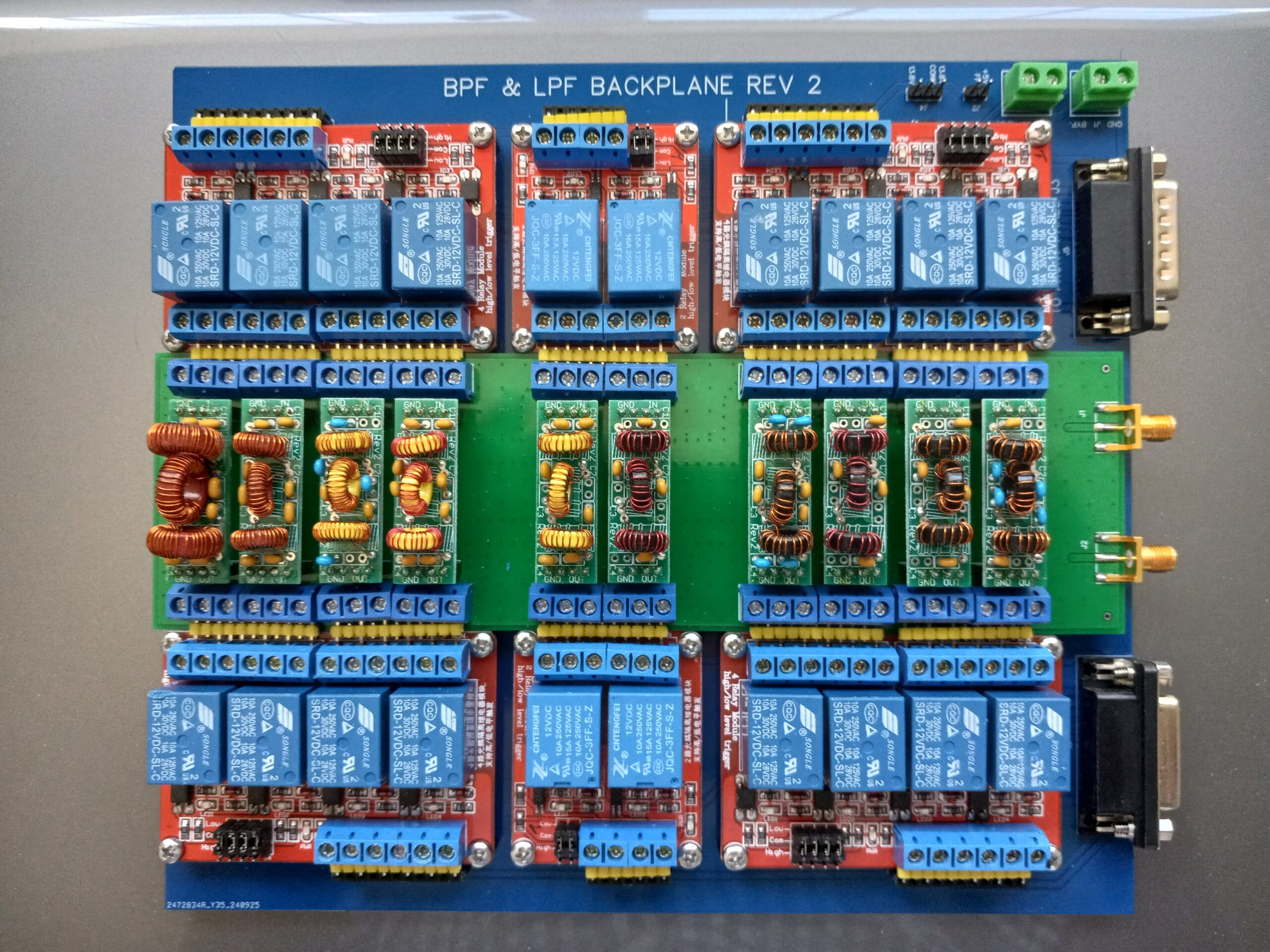 Figure 3. Lowpass Filter Backplane. The Lowpass Filter Backplane provides all of the relay interconnects for power and logic signals. All of the logic connections for filter selection are brought out to a pair of subminiature-D connectors at the right end of the Backplane. The D connector in the upper left corner receives logic commands for filter selection from the Arduino. The subminiatue-D connector at the lower right is used to jumper logic signals to the Bandpass Filter Backplane Assembly that resides in the layer above it. DC power is brought to a screw terminal strip at the upper right corner of the backplane. A second screw terminal strip is provided for Receive Bypass BCI Notch Filter connection. Please click on the figure to open it in a new window.
Bandpass Filters and Image Rejection
This section will describe how bandpass filters may be used to improve image rejection in a single conversion receiver.
An Image is an unwanted signal that resides at a separation in frequency equal to the signal frequency from the local oscillator signal. It may be equidistant, above or below the local oscillator signal. In Figure 4, it resides below the local oscillator signal. The unwanted image, when mixed with the local oscillator signal, will produce a signal at the same Intermediate Frequency (IF) as the wanted signal. If there is a strong signal at the unwanted image frequency, which is frequently the case, the wanted signal will be clobbered.
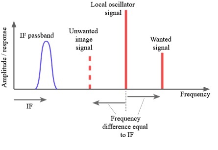 Figure 4. Image Frequency. There exists an unwanted frequency spaced equidistant from the LO frequency that can also mix to IF, as is shown in the figure. In the absence of an additional conversion stage or an image reject mixer, a bandpass filter around the desired signal is generally used to suppress this unwanted image signal. Figure from Electronics Notes, Ian Poole, author. Please click on the figure to open it in a new window.
In order to avoid the complexity of additional conversion stages or the expense of image reject mixers, a bandpass preselection filter is often added to the design to prevent some of the image frequency power from entering the receiver in the first place. It’s not perfect, but it is better than nothing.
Bandpass Filters
So, what is a bandpass filter? A bandpass filter is an active or passive device that limits the input power to a circuit to a predetermined bandwidth. One might think of a bandpass filter as a highpass filter that admits only higher frequencies while rejecting lower frequencies to which has been added a lowpass filter that admits lower frequencies while rejecting higher frequencies. An example of how one might be synthesized is shown in Figure 5 [21].
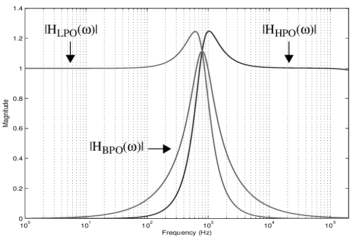
Figure 5. Bandpass Filter Response. The response of a lowpass filter, HLPO, as combined with the response of a highpass filter, HHPO, to form a bandpass filter, HBPO. Please click on the figure to open it in a new window.
Bandpass Filter and Receiver Noise Floor
There is an added benefit to adding a bandpass filter to the receiver design. The desired receive signal power often resides in a bandwidth of no more than 3 kHz. Noise of many varieties resides over a much greater power bandwidth. This noise competes with the signal at the receiver input. If the input bandwidth of the receiver is narrowed to that necessary to admit a narrower band of signals, the amount of noise power entering the receiver is greatly reduced. Often, a signal that has been “buried” in noise becomes detectable.
This is only part of the story, however. The receiver will generate electronic noise of more than one type, and some care in design is required to reduce any additional receiver noise. A property that affects the ability to pull a signal out of noise is the Noise Figure (NF) of the receiver. Notable contributors to degraded Noise Figure are the losses that precede the semiconductor amplifiers, such as attenuators, conductor resistance, and filter losses. These pile on additional noise before we get to the active elements of the receiver. Once we add in the amplifier portion of Noise Figure and any additional bandwidth limiting, we arrive at something called the Minimum Detectable Signal (MDS). That is how small the signal may be as compared to the noise power in the ultimate, filtered bandwidth of the receiver.
The MDS also contributes to something called the Spur Free Dynamic Range (SPDR) of the receiver. In order to calculate it, we need to know something called the Third Order Intercept (TOI, also called IP3) point of the receiver. That is measured by injecting two non-harmonically related, equal amplitude, closely spaced signals into the front of the receiver. The resulting Third Order products (2F1-F2 and 2F2-F1) are plotted against that of the fundamental signals. If we extrapolate the straight sections of both plots, we reach a point of intersection. The point where the two intersect is called the TOI, Figure 6. That point, for small signal amplifiers, is typically 16 dB above the 1 dB compression point.
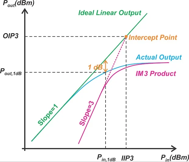
Figure 6. Third Order Intercept Point Determination. As a rule of thumb, and for small signal amplifiers, the Third Order Intercept Point will reside about 16 dB higher than the amplifier’s 1 dB compression point. The 1 dB compression point is defined as the output power level for which any 1 dB incremental increase in the input power level produces an output power that is 1 dB less than is expected, i.e., it is 1 dB compressed. Graphic from All About Circuits, Steve Arar. Please click on the figure to open it in a new window.
For this receiver, all of the system parameters from the Stockton Bridge backwards have been considered. The Qorvo Cascade Analysis Calculator [22] was employed to compute the cascaded receiver gain, noise figure, 1 dB compression point, and the Third Order Intercept Point. The ultimate bandwidth of the signal channel is set by the crystal bandpass filter to 2.7 kHz. The NF for this receiver is 7.8 dB, the MDS is -131.9 dBm (Figure 7) the TOI is +12.1 dBm, and the Spur Free Dynamic Range (SFDR) is 96 dB. The SFDR suffers from the small bias currents primarily in the amplifier stages [23]. These amplifiers were designed by Wes Hayward and Bob Kopski to conserve battery power for portable QRP use. A later iteration improves upon the amplifier performance [24]. Even though this SFDR departs from the current state-of-the-art of well over 100 dB, the result represents something that is highly gratifying.
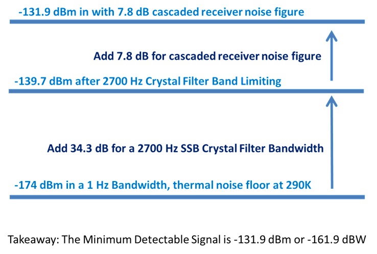
Figure 7. The Minimum Detectable Signal. Since the thermal noise floor at 290K is -174 dBm in a 1 Hz bandwidth, that is the starting point. This is degraded by the width of the crystal filter in the radio that degrades the noise bandwidth to 2700 Hz, which converts to 34.3 dB. This admits more noise into the receiver input, and the noise floor increases from -174 dBm to -139.7 dBm. The receiver is not noiseless, and it has a cascaded noise figure of 7.8 dB. This degrades the noise floor even further to -131.9 dBm, which is the MDS for our receiver.
MDS and SFDR Calculations
Minimum Detectable Signal (MDS) = -174 dBm (in a 1 Hz bandwidth) + NF(dB) +10 log ( xtal filter bandwidth in Hz)
MDS = -174 dB + 7.8 dB + 10 log (2700) = -131.9 dBm in a 2700 Hz Bandwidth
Spur Free Dynamic Range (SFDR) = 2/3 [IP3- MDS]
SFDR = 2/3[12.1- (-131.9)] = 96 dB
Bandpass Filter Source of Supply
Since the bandpass filter kits from QRP Labs [25] were built, assembled into a filter bank, and tested in 2008, they have not been retested. Recently, a spectrum analyzer with an integral tracking generator was used to re-sweep the passbands of all 10 filters. Adjustments were made as necessary.
Bandpass Filter Assembly
Nearly 8 years ago, the Bandpass Filter Assembly was completed, Figure 8. Arduino relays were chosen for switching the filters in and out of the circuit because of their ease of use. That turned out to be prophetic. The only downside of Arduino relays is that they are power relays, not signal relays. Over time they develop contact resistance through oxidation. This may be mitigated by passing a small DC current, say 20 mA, through the relay contacts to break up the oxidation. If injected with something called a Bias-T, the signal will pass unaffected through the Bias-T and the selected bandpass filter.
 Figure 8. Bandpass Filter Assembly. The Bandpass Filter Bank as it appeared 8 years ago. It was lacking an interconnection backplane for logic connections and DC. The SMA launchers are soldered to the end of coplaner waveguides that reside on the bottom side of the green circuit card. Please click on the figure to open it in a new window.
Bandpass Filter Backplane
The means for connecting 10 bandpass filters to DC relay power and logic was not completed until 2024. The completed assembly is shown in Figure 9. Places for two subminiature-D connectors are provided. Only one is required for the bandpass filter because it receives its logic signals through a jumper cable from the Lowpass Filter Backplane stacked beneath it .
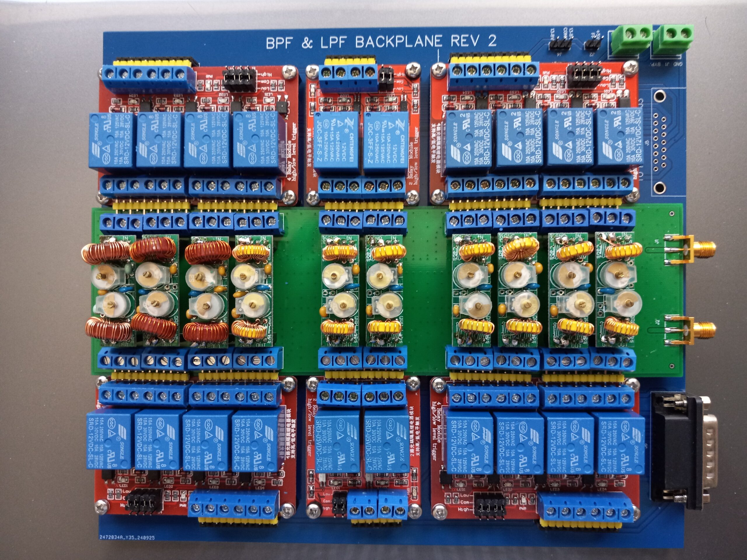 Figure 9. The Bandpass Filter Bank As It Resides On an Interconnection Backplane. All of the logic signals for filter selection are brought out to a single subminiature-D connector at the lower right-hand corner. RF travels via the SMA connectors. DC power is brought to a screw terminal strip at the upper right corner of the backplane. A second screw terminal strip is provided for the Receive Bypass BCI Notch Filter connection. Please click on the figure to open it in a new window.
Broadcast Interference (BCI) Notch Filter
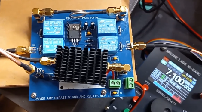
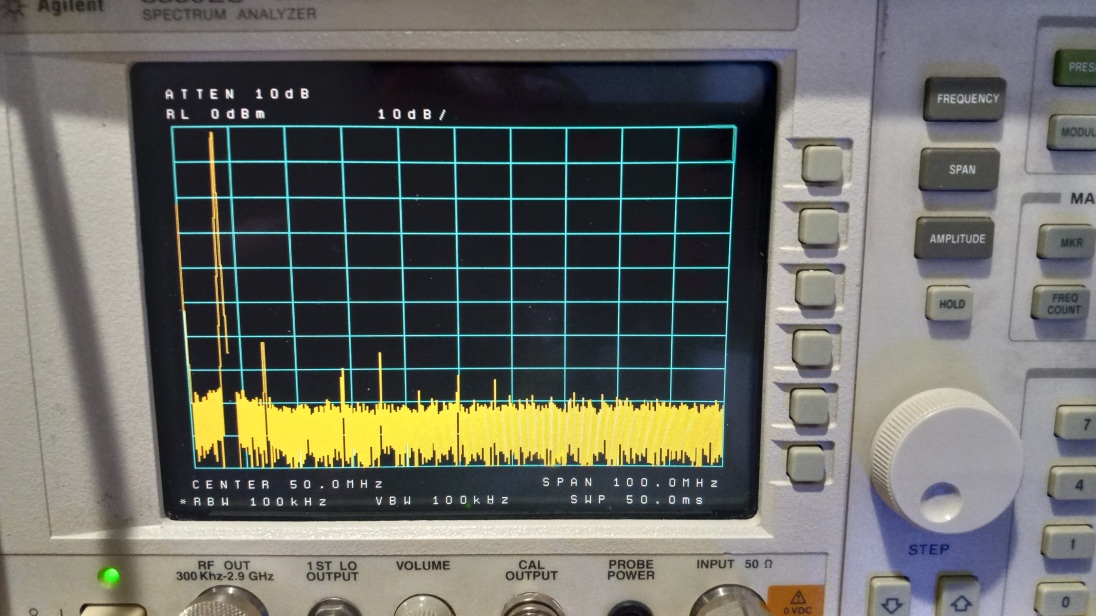
A BCI Notch Filter manufactured by Nooelec [26] is used in the receive bypass path as described earlier in this paper to reject strong AM broadcast stations by 70 dB when the receiver is tuned to shortwave band segments other than the ham bands. The Receive Bypass BCI Notch Filter Assembly is shown in Figure 10, while the Nooelec specified notch performance is shown in Figure 11. Finally, the measured performance is shown in Figure 12.
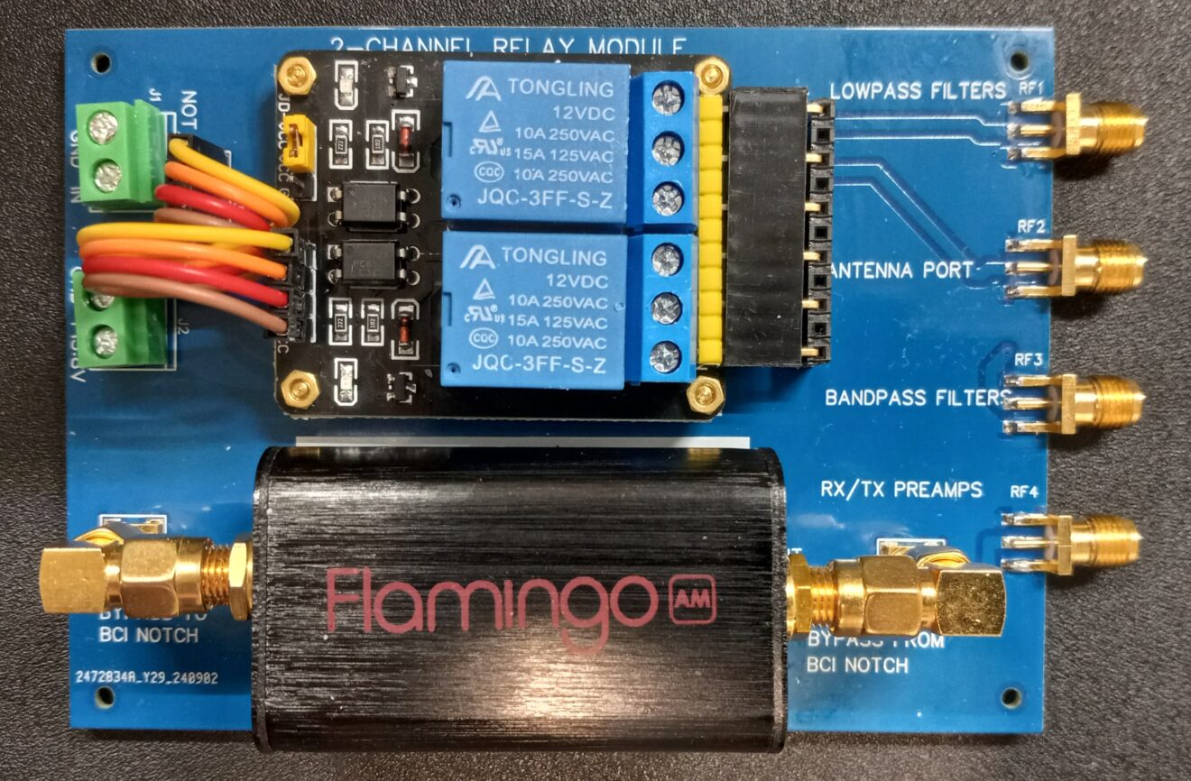
Figure 10. Receive Bypass BCI Notch Filter Assembly. This module provides the means necessary to switch a receive bypass in place of the lowpass and bandpass filters when the receiver is tuned to general coverage bands other than the ham bands. Figure 1 shows where in the receiver the Receive Bypass BCI Notch Filter Assembly resides. The BCI Notch Filter is manufactured by Nooelec. Please click on the figure to open it in a new window.
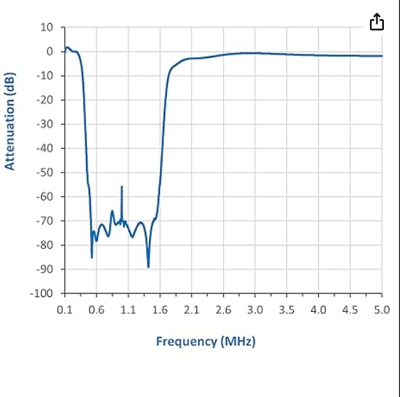 Figure 11. The Specified Nooelect BCI Notch Filter Performance. The BCI notch is nearly 70 dB deep over the entire AM broadcast band. Please click on the figure to open it in a new window.
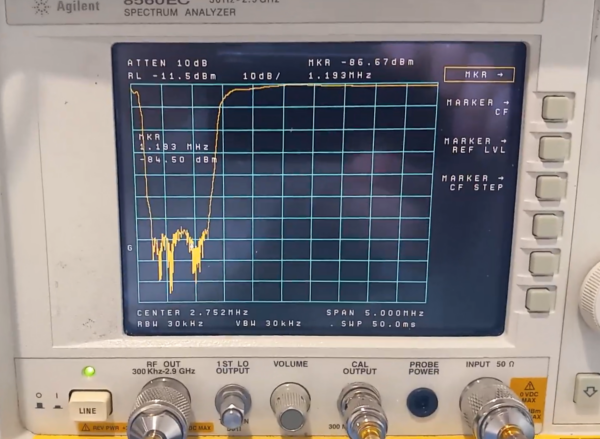
Figure 12. Measured Nooelec BCI Notch Filter Performance. The module was evaluated on a spectrum analyzer. The performance of the notch is impressive and matches its specified AM band rejection closely. It is nearly 70 dB over most of the broadcast band. Please click on the figure to open it in a new window.
Control Panel and Front Panel Integration
Recently, I summoned the courage to stack the Control Panel Module with the Arduino Front Panel Module, Figure 13. That operation proceeded smoothly. The only thing that I wish had been planned better was the location of a subminiature-D connector that connects the front panel to the control panel. The connector for the Front Panel Module interconnects is on the upper left side of the stackup, while the connector for the Control Panel Module interconnects is on the upper right side of the stackup. This necessitates a rather long interconnect cable between the two. A subsequent iteration of the front panel layout should remedy this.
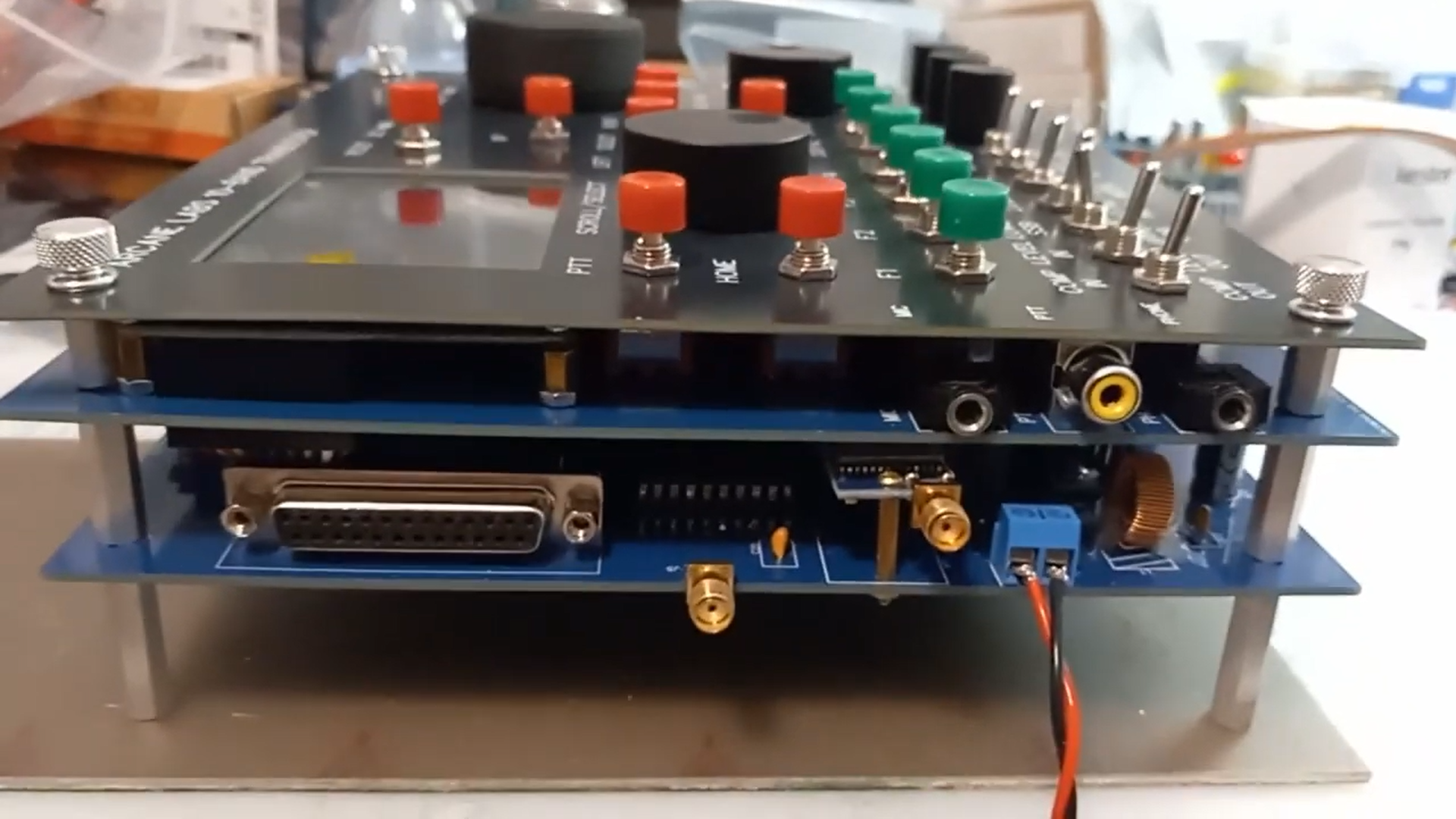 At a) the left hand view showing the subminiature-D connector from the Arduino Front Panel to the Control Panel layer above it, GPS antenna input, the 10 MHz frequency reference input, +13.8 VDC Input, Mic Input, Push-to-Talk Input, and Headphone Output.
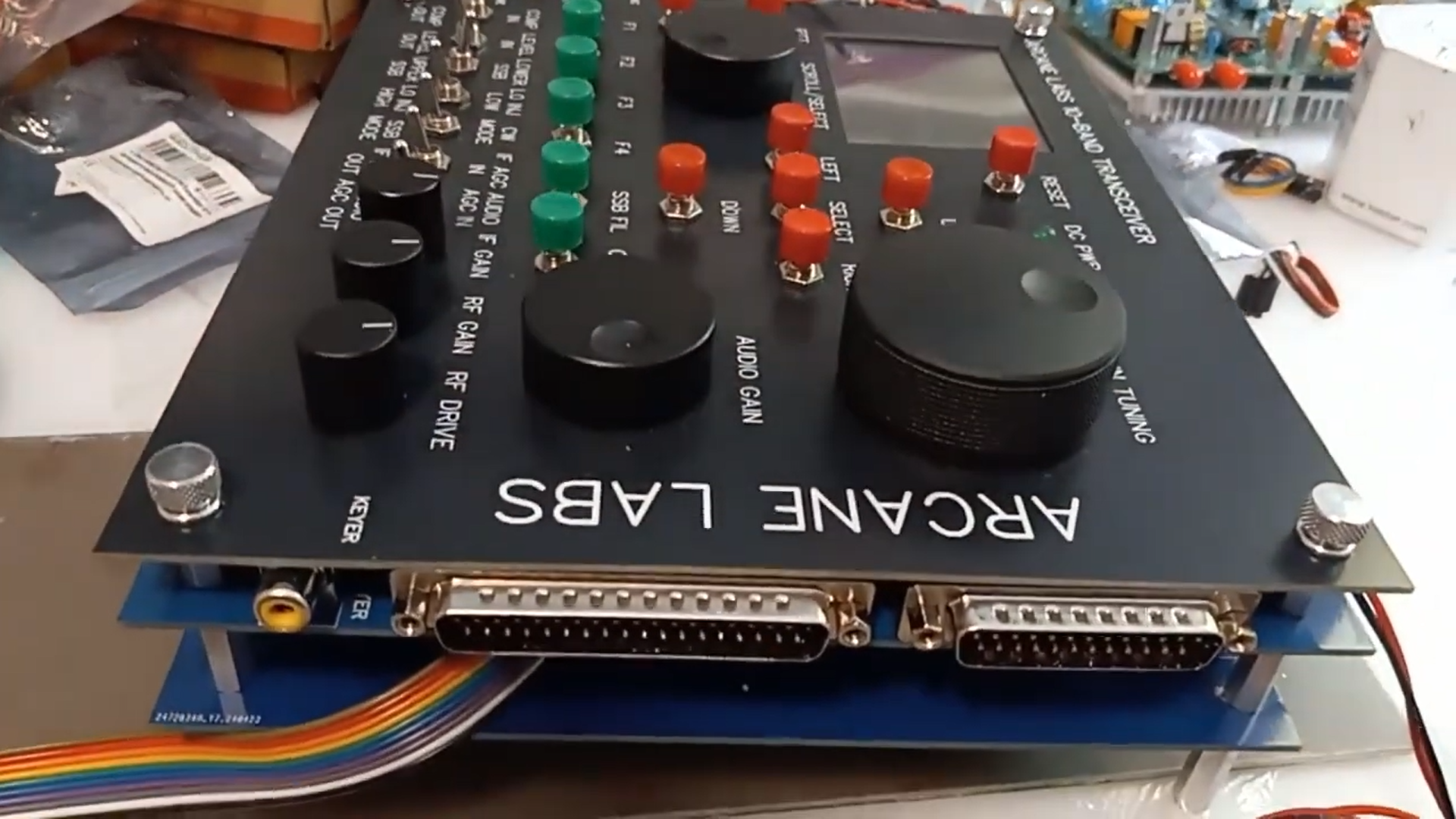 At b) the right hand view showing, to the left, the subminiature-D connector to interface with various radio functions controlled by the Control Panel and, to the right, the subminiature-D connector that interfaces with the Arduino Front Panel layer beneath it.
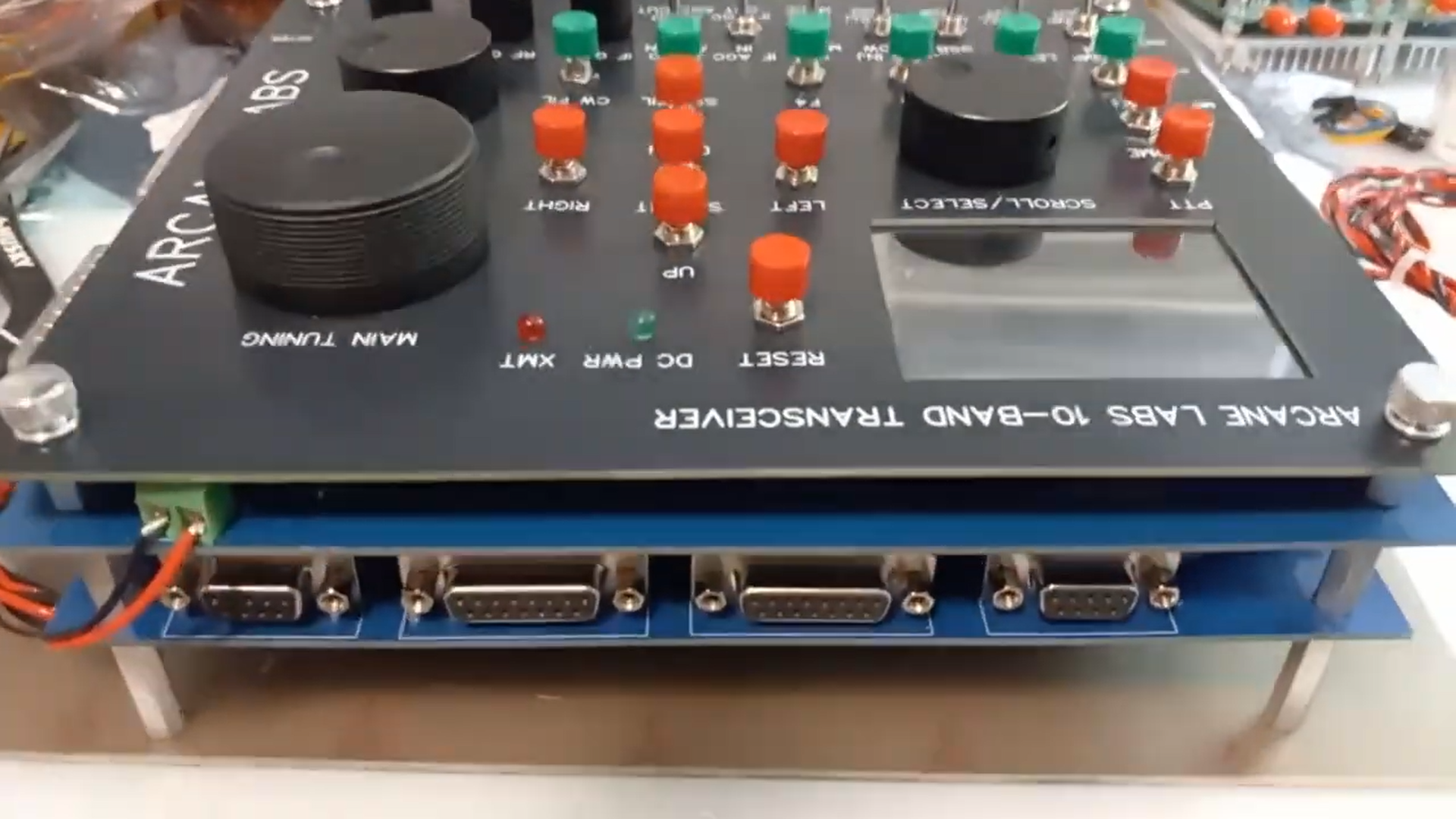 At c) the top view showing, to the left, the subminiature-D connector that interfaces to the transmitter temperature sensors and to the Stockton Bridge Module. Second from the left, the subminiature-D connector that interfaces to the lowpass and bandpass filters. Third from the left, the subminiature-D connector that interfaces to the RF deck. Finally, fourth from the left, is access to Arduino spare I/O.
Figure 13. Control Panel Escutcheon, Control Panel and Arduino Front Panel Integration Views from 3 Sides. All of these PCB layers were of similar dimensions which made stacking easy. I breathed a sigh of relief that nothing was damaged. Please click on each figure to open it in a new window. At a) left view, at b) right view, and finally at c) top view.
Integration of Bandpass and Lowpass Filters with the Control Panel and Arduino Front Panel
Once the bandpass filters had been retuned, the Lowpass Filter and Bandpass Filter Backplanes were stacked behind the Control Panel and Front Panel, Figure 14. This required an aluminum adapter plate between the Arduino Front Panel layer and the Bandpass Filter Backplane layer. In addition to providing a mechanical interface, this plate serves to provide some measure of digital noise shielding between the Arduino and the bandpass filters.
While it does not by any means demonstrate performance, a YouTube video [27] was made to demonstrate how band switching commands are asserted by Arduino software to detect ham band tuning and to select the corresponding bandpass and lowpass filters.
For general coverage, all of the filters are bypassed and a Broadcast Interference (BCI) Notch Filter is inserted in place of both filter banks.
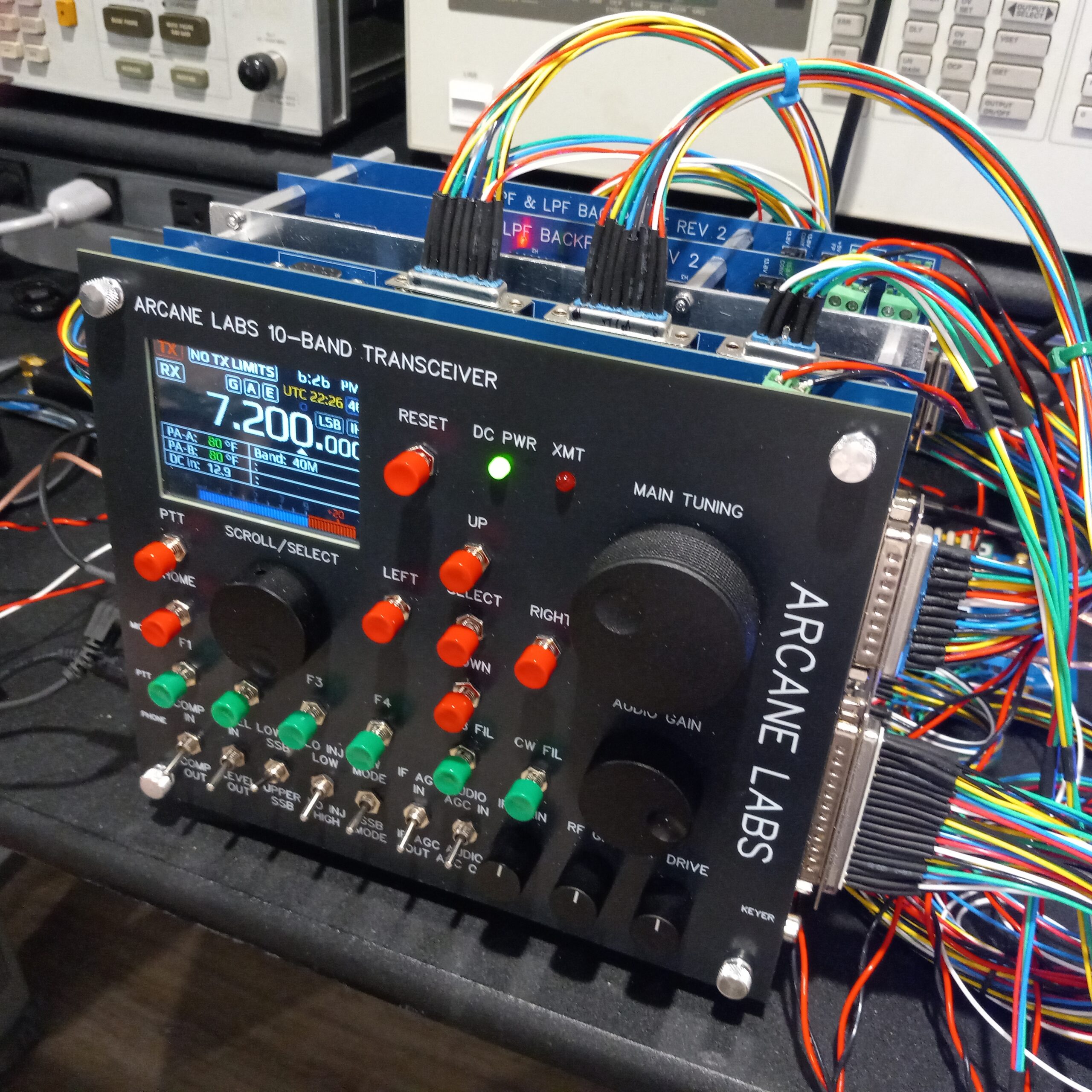 Figure 14. Control Panel, Front Panel, Bandpass Filter and Lowpass Filter Level of Integration. Several modules are shown stacked, one behind the other – Control Panel escutcheon first, Control Panel second, Arduino Front Panel third, Shielding fourth, Bandpass Filters fifth, and Lowpass Filters sixth. Please click on the figure to open it in a new window.
Breadboard Receiver Integration
It has been more than 2 years since a rudimentary breadboard receiver was strung together on the bench. No band preselection filters were present at the time. Nonetheless, both CW [28] and SSB signals [29] were received on the 40m band. The audio was of questionable quality because of the switching power supply (power supply ripple abounds) and the 6-foot piece of wire used as an antenna.
Having been satisfied that everything was still working following filter integration; the remainder of the RF and IF modules were collected and temporarily fastened to the workbench with blue masking tape to prevent them from sliding around, Figure 15. These included an RF to IF Converter Module without AGC, a Crystal Filter Module, an IF to Baseband Module, an SI5351 Clock Generator Module, a breadboard 1W Audio Amplifier Module, and a Power Management Module. The Receive Bypass BCI Notch Filter Module was not used.
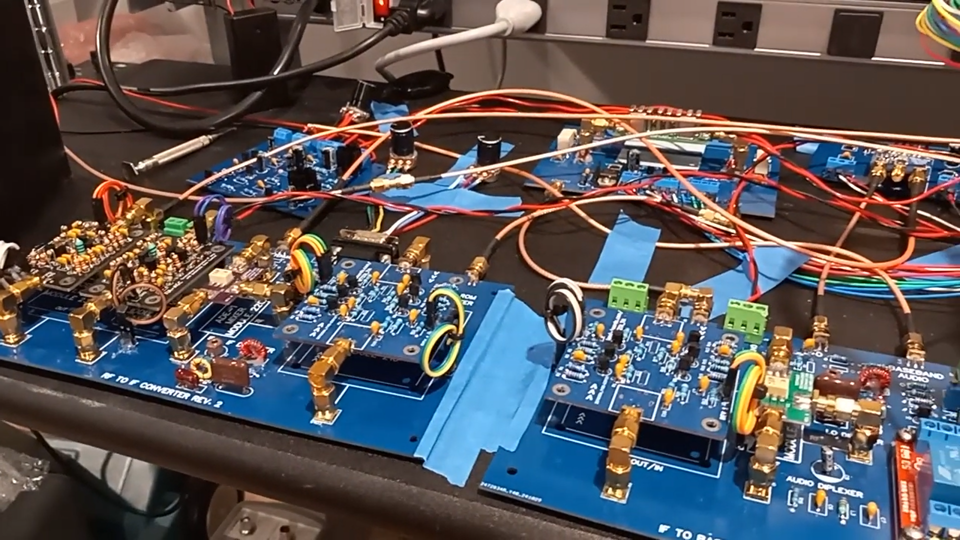 At a) just enough of the receiver modules to make it work – top left, the Audio Amplifier Module; top middle, the Crystal Filter Module; top right, the SI5351 Clock Generator Module; bottom left, the RF to IF Converter Module; bottom right, the IF to Baseband Converter Module.
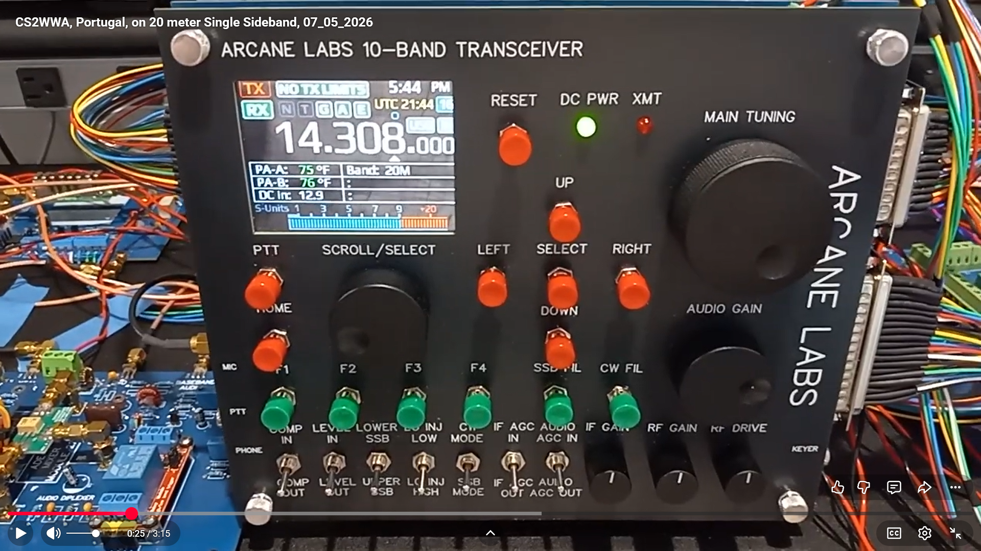 At b) a view of the control panel escutcheon with display and controls. The radio is tuned to Portuguese station CS2WWA in contest.
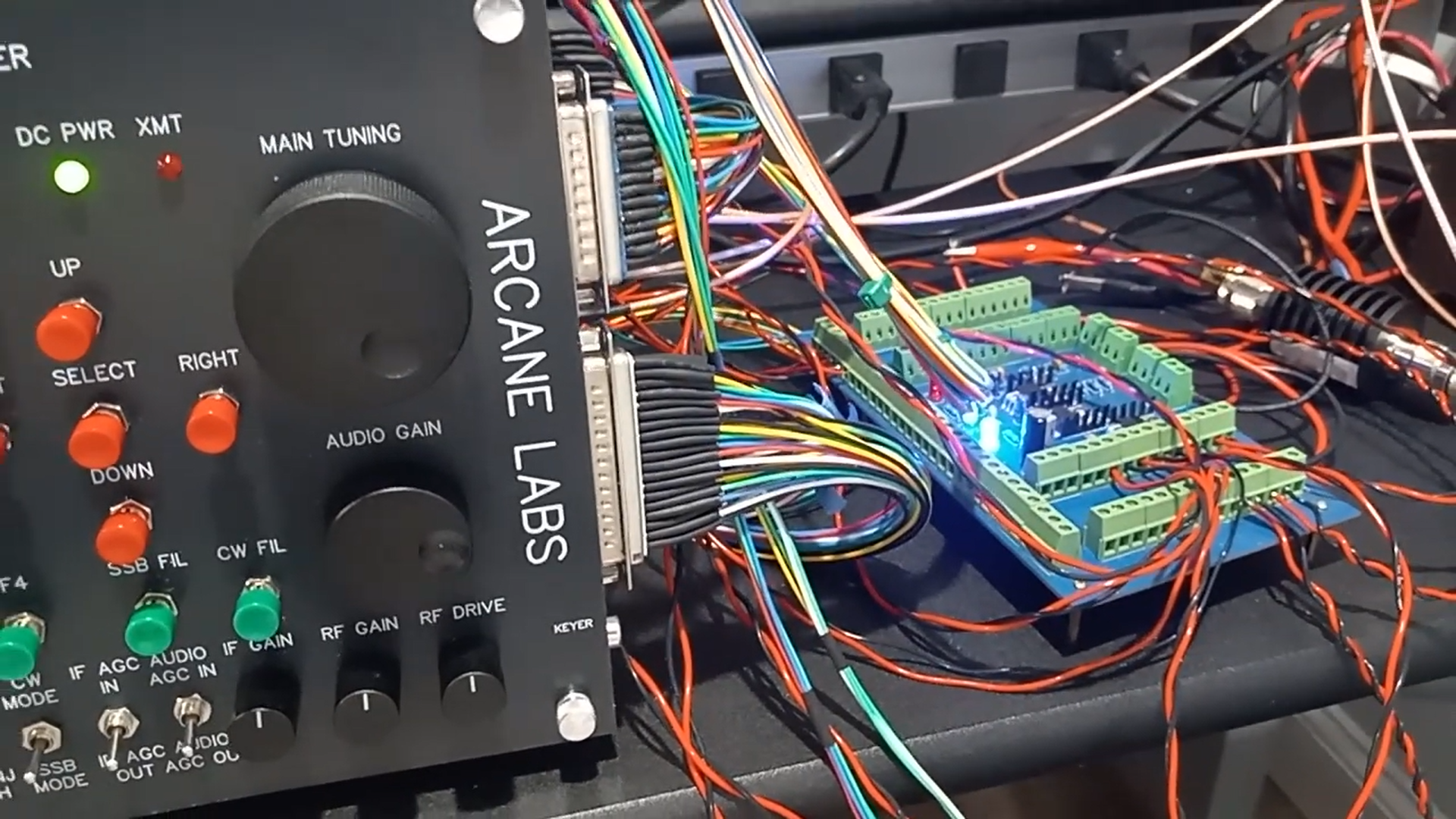 At c) the Power Management Module. This module makes use of power MOSFETs for transmit/receive switching. Separate screw terminals for transmit, receive, and continuous power make +13.8 VDC power integration easy.
Figure 15. Receiver Integration Test Setup. All of the receiver modules were spread out and anchored to the test bench with blue masking tape. The Control Panel Escutcheon has already been fully integrated with the Control Panel Module, the Arduino Front Panel Module, the Bandpass Filter Backplane Module, and the Lowpass Filter Backplane Module. At a) top left, the Audio Amplifier Module; top middle, the Crystal Filter Module; top right, the SI5351 Clock Generator Module; bottom left, the RF to IF Converter Module; bottom right, the IF to Baseband Converter Module. At b) the Control Panel Escutcheon. At c) to right, the Power Management Module. Note that the Receive Bypass BCI Notch Filter Module was not integrated for this test. Please click on the figure to open it in a new window.
RF to IF Converter Module
The RF to IF Converter Module, Figure 16, was described in detail in a separate article [30]. Two W7ZOI amplifiers are wired bidirectionally to the left side of the photo, one for receive and one for transmit. The gains of these amplifiers may be varied by application of an AGC voltage that is generated by potentiometers on the Control Panel. Thus, one of the potentiometers serves as an RF gain control for receive, and the other serves as the RF drive gain control for transmit. The amplifiers were sourced from Mostly DIY RF [31], and they function perfectly. A doubly balanced mixer is at the center of the photo. It consists of a connectorized Mini Circuits ADE-1 mixer [32] that requires +7 dBm VFO drive level from the SI5351 clock generator [33]. Since the clock generator output impedance is greater than 50 ohms, a transformer is provided to step the impedance down. A bridged-T diplexer, tuned to 9 MHz, terminates the IF port of the mixer to ensure that the mixer sees 50 ohms at the IF frequency. Mixers work as specified when they are properly terminated. Please note that the Termination Insensitive Amplifiers (TIAs) that precede the mixer ensure a 50 ohm match to the RF port of the mixer. Since the LO port is tuned over a wide tuning range, all we can do is make sure that the SI5351 clock generator has been properly transformed to 50 ohms. Finally, a bidirectional, fixed-gain, Termination Insensitive Amplifier is provided at the module output. It was sourced from land-boards.com [34].
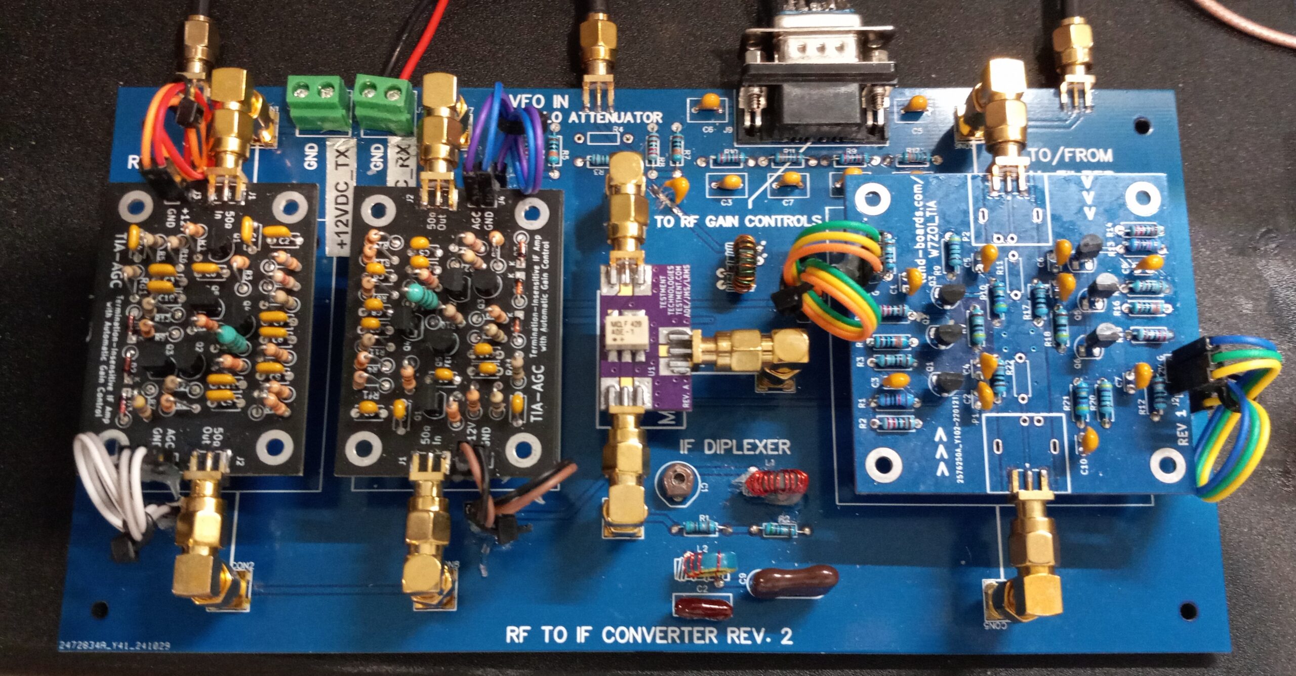
Figure 16. Closeup of the RF to IF Converter Module Without AGC. An RF to IF Converter Module was designed without RF AGC in order to provide a receiver demonstration more quickly. A second RF to IF Converter with RF AGC will be integrated into the receiver in the future. This module contains two amplifiers of W7ZOI design with manual gain control at RF that have been wired bidirectionally for transmit and receive. This is followed by the first conversion mixer stage to convert RF to 9 MHz upon receive and 9 MHz to RF upon transmit. The mixer is tuned by the SI5351 clock generator that acts as a VFO. Finally, a fixed-gain, bidirectional amplifier is provided for additional gain at 9 MHz. Please click on the figure to open it in a new window.
Crystal Filter Module
The Crystal Filter Module was described in detail in a separate article [35] to be submitted at a future date. The module, Figure 17, is controlled from the Control Panel by two push-button switches – one for CW and another for SSB. The tiny, white signal relays on the board are of the magnetic latching type. Once they are pulsed to either state, they will stay in that state even if power is removed from the relay coils. There are also spaces on the board for matching transformers if matching is not provided on the crystal filters. This feature provides a means to mix and match different types of filters in the same module. For example, the SSB filter in the photo requires external matching while the CW filters, for which there is a space, do not.
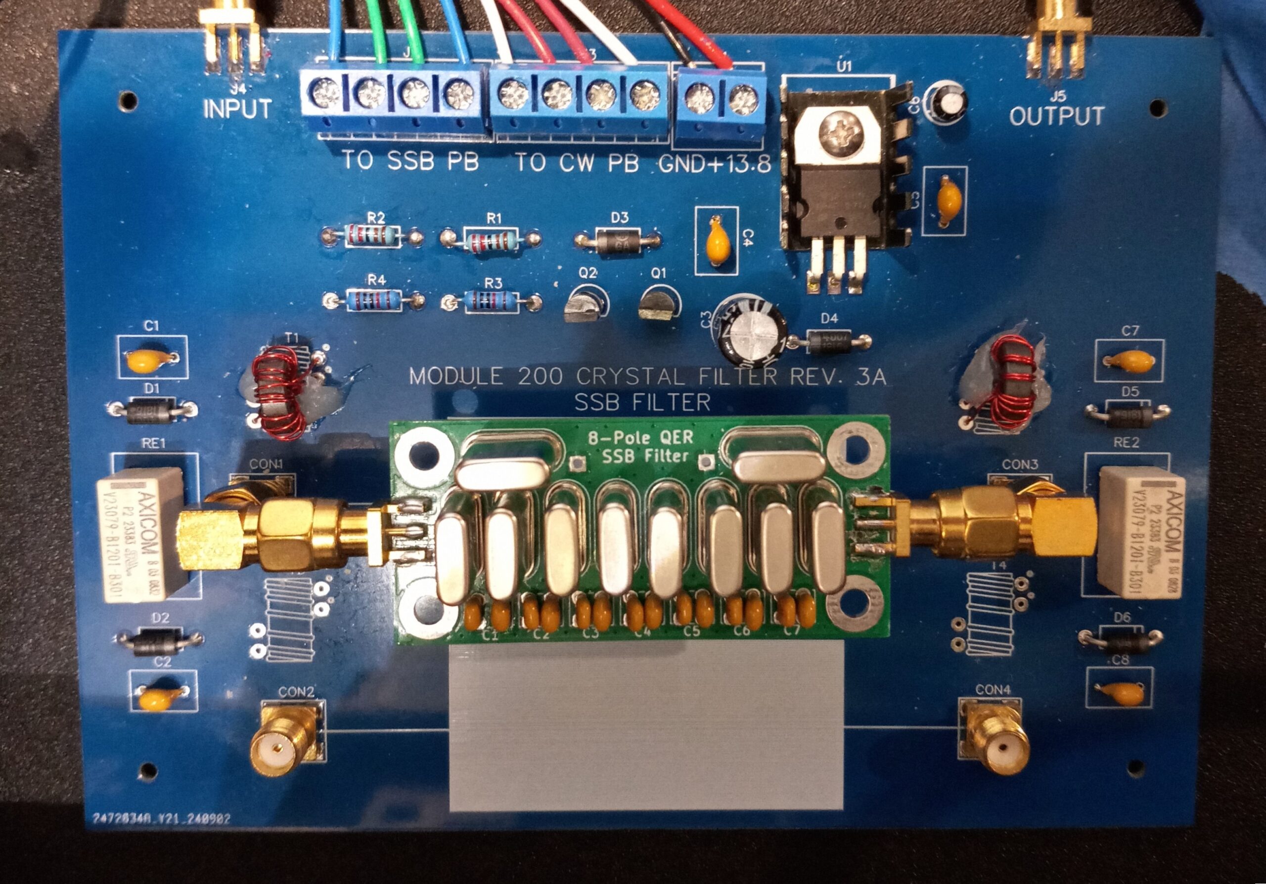 Figure 17. Closeup of the Crystal Filter Module. A QER 8-pole crystal filter from Mostly DIY RF provides unwanted sideband rejection for transmit as well as bandwidth control. Similarly, upon reception, it provides frequency selectivity. The PCB provides spaces for crystal filter matching transformers in the event that they have not been provided on the filter PCB. For the case of the SSB filter, the transformers had not been provided and had to be provided externally. There is also a space on the PCB for a CW filter that had not been installed at the time of the photo. Please click on the figure to open it in a new window.
The as-built performance of the 8-pole quasi-equiripple (QER) SSB crystal filter is shown in Figure 18. The bandwidth is 2700 Hz while the insertion loss is just 2.5 dB. The filter was sourced from Mostly DIY RF [36], and the quality is excellent. The proof is in just how good the radio sounds.
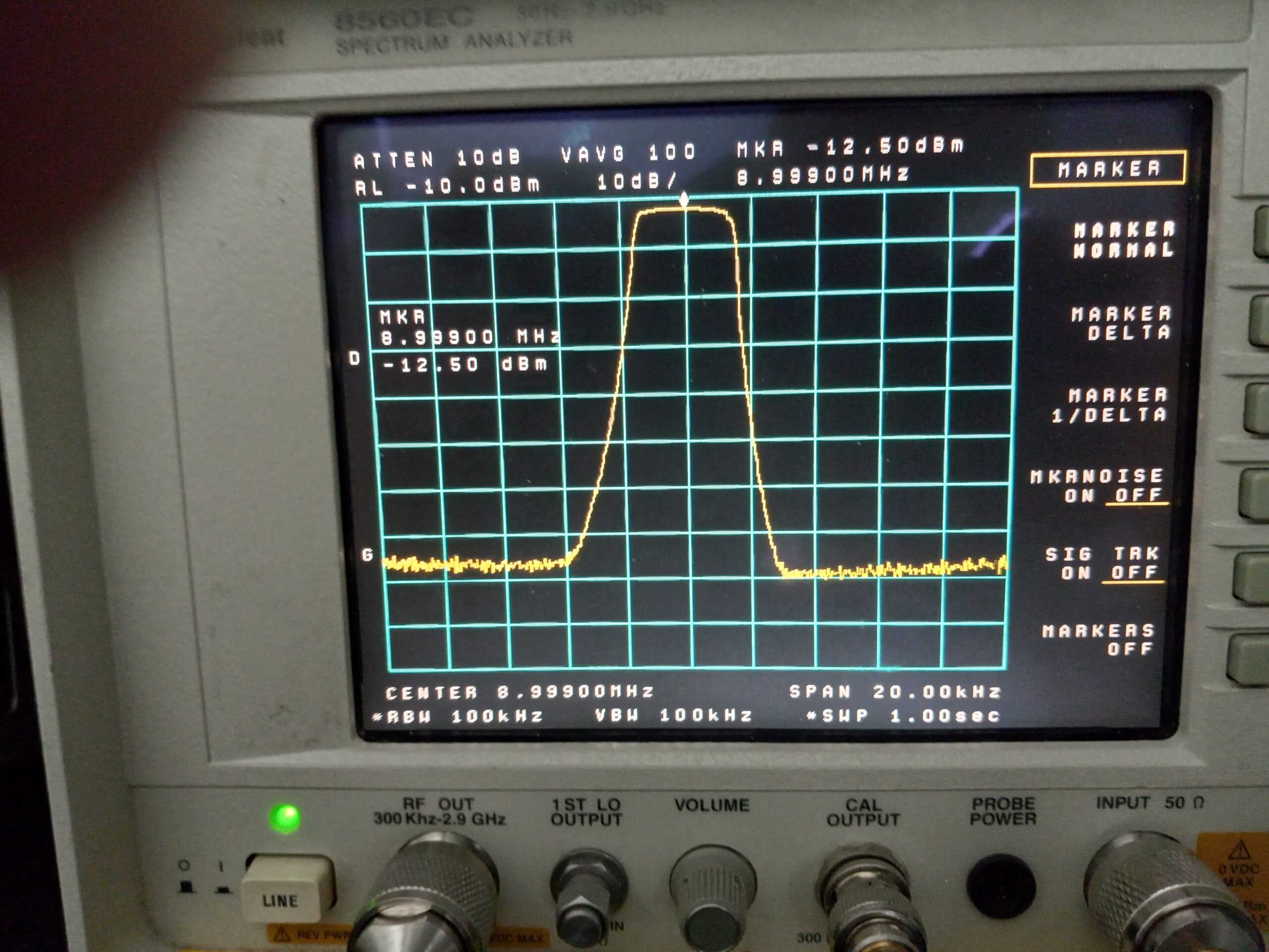 Figure 18. Crystal Filter Performance. This 8-pole Quasi-Equiripple (QER) filter was manufactured by Mostly DIY RF, and I couldn’t be happier with it. Making good crystal filters is an art, and Todd Carney, K7TFC, has mastered it. The bandwidth is 2700 Hz, and the loss is 2.5 dB. Please click on the figure to open it in a new window.
IF to Baseband Converter Module
The IF to Baseband Converter Module, Figure 18, was described in detail in another article [37]. Another fixed-gain, bidirectional, Termination Insensitive Amplifier (TIA) is placed at the input of the module. It was sourced from land-boards.com [38]. This is followed by another connectorized Mini Circuits ADE-1 Mixer [39] requiring +7 dBm of local oscillator (LO) drive. This time it is the BFO signal that is the LO. Since the BFO frequency is fixed and close to 9 MHz, a bridged-T diplexer terminates the LO port of the mixer The RF port of the mixer is terminated by the 50-ohm inputs/outputs of the bidirectional TIA. That leaves the IF port, which is terminated at audio frequencies by an audio diplexer that first appeared in a paper by Roy Lewallen, W7EL [40].
Since the IF to baseband converter module’s ADE-1 mixer will also be used as a balanced modulator on transmit, an LM723-based millivolt power supply has been provided whose purpose it is to unbalance the balanced modulator so that a carrier may be reinserted for tuning the radio into an antenna.
The combination of RF diplexers, audio diplexers, and the TIAs on all mixer ports result in superior carrier suppression for SSB generation.
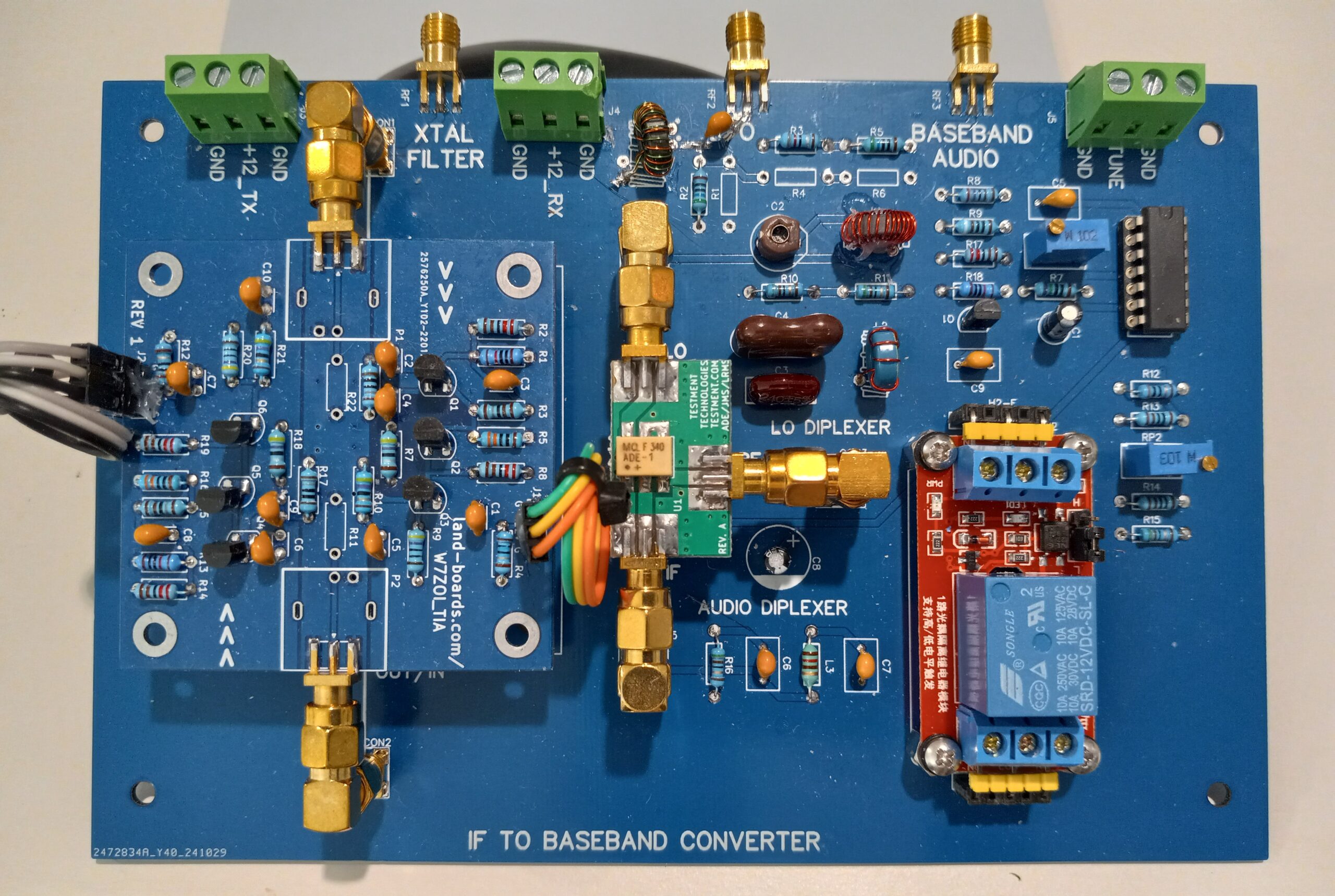 Figure 18. Close-up of the IF to Baseband Converter Module. An IF to Baseband Converter Module was designed that makes use of the Si5351 Clock Generator at a fixed IF frequency close to 9 MHz. The first stage is a bidirectional amplifier at 9 MHz of the W7ZOI design followed by a doubly balanced mixer that accepts the BFO frequency to convert the 9 MHz IF frequency to baseband audio upon receive. Upon transmit, the doubly balanced mixer acts as a balanced modulator to generate SSB. A precision DC mV power supply, also on the board, is used to unbalance the mixer, which acts as a balanced modulator, upon transmit. In so doing, a carrier is injected into the transmit path to tune the radio into an antenna. Please click on the figure to open it in a new window.
SI5351 Clock Generator Module
The SI5351 in Figure 19 is used to generate the VFO, the BFO, and a 10 MHz signal for SI5351 25 MHz master clock calibration. This calibration signal is available on the Clock 1 connector. It works in combination with the 1 PPS signal generated by a GPS receiver located on the Arduino Front Panel to calibrate the 25 MHz clock to great accuracy. This calibration process is accessible from drop-down menus on the display. Once calibration has been completed, the 10 MHz clock may be turned off so that it does not interfere with normal receiver operation, in particular, the 10 MHz WWV signal. The SI5351 clock generator was sourced from Adafruit [41]. The only other thing included on this module is a +5 VDC regulator.
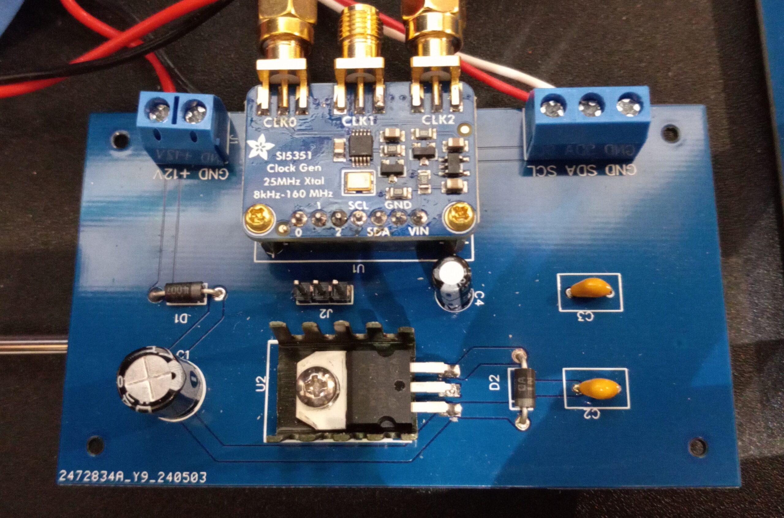 Figure 19. Close-up of the SI5351 Clock Generator. This frequency synthesizer can produce three signal outputs at three different frequencies at the same time. One of the three outputs acts as the VFO for both receive and transmit. A second BFO output generates a signal close to 9 MHz that serves to convert the IF frequency to baseband audio. A third output is set to 10 MHz. Its function is to calibrate the SI5351 crystal clock to exactly 25 MHz against a 1 PPS GPS signal. This signal originates in the GPS receiver module located on the Arduino Front Panel PCB layer. Please click on the figure to open it in a new window.
Breadboard Audio Amplifier Module
This Class AB audio amplifier [42], Figure 20, was built for test purposes 2 years ago. To improve the output power and heat dissipation, the output devices were changed to venerable 2N2905’s and 2N2219’s in TO-5 cans. The circuit employs a 2N7000 for muting to prevent popping and crackling when the transceiver is switched to and from receive. An adjustment potentiometer is used to minimize crossover distortion in Class AB operation. The output pair produces just short of 1W of room-filling loudspeaker volume. An even more powerful Class AB amplifier is included on the Multifunction Audio Processor Module. In the finished radio, a Rick Andersen, KE3IJ (SK), general-purpose amplifier will drive an audio leveling circuit, which will, in turn, be followed by an even larger Class AB power amplifier.
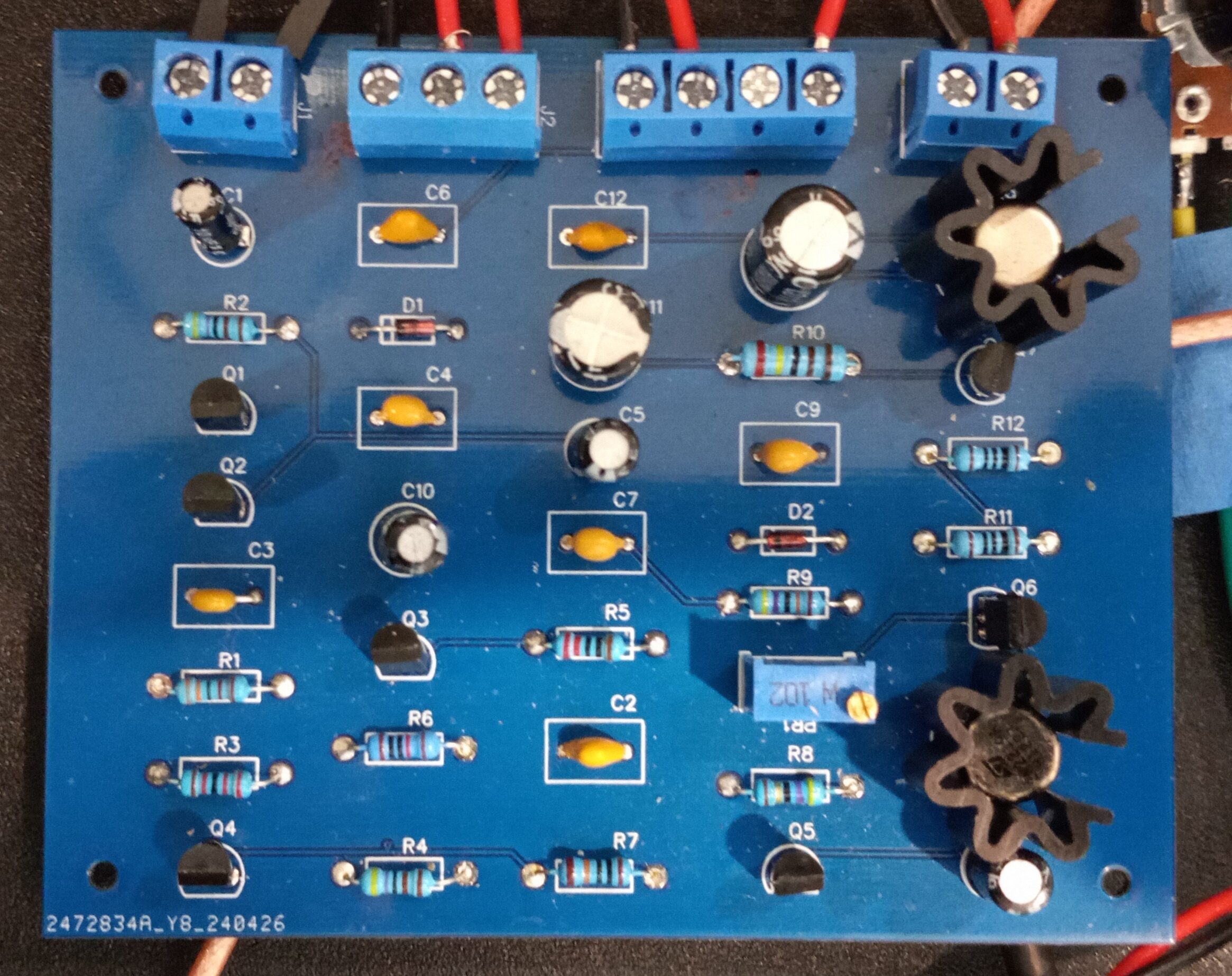 Figure 20. Close-up of the Breadboard Audio Amplifier. A breadboard push-pull audio amplifier was built and tested prior to integration into the Multifunction Audio Processor PCB, not shown. This discrete audio amplifier is capable of producing somewhat less than 1W of audio. It produces low-distortion, room-filling loudspeaker volume. A Rick Andersen, KE3IJ (SK), amplifier replaces this one on the Multifunction Audio Processor Module to drive an audio leveling circuit which, in turn, drives an even larger Class AB audio power amplifier. Please click on the figure to open it in a new window.
Power Management Module
The Power Management Module [43], Figure 21, ensures smooth switching from receive to transmit. It uses low Rds ON Vishay SUP60061EL power MOSFETs that have been tested to 30W with a power resistor load. At 30W, the power MOSFET devices run slightly warm.
This module provides all of the DC voltages required to power the transceiver. When push-to-talk is asserted, the transmit screw terminals are powered ON and the receiver terminals are powered OFF. There is also a set of screw terminals for continuous DC power for those modules that run continuously. This circuit has been indispensable for transceiver integration.
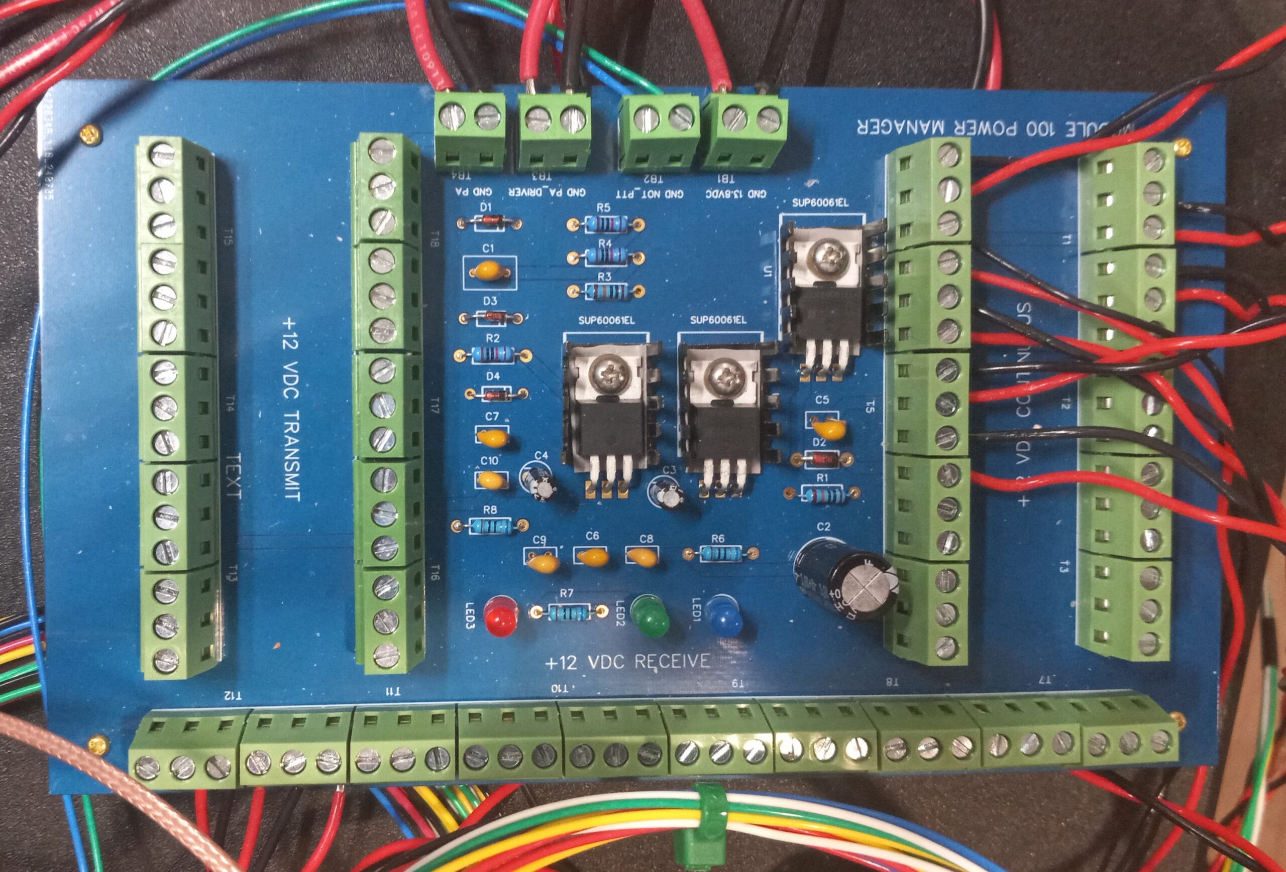
Figure 21. Close-up of the Power Management Module. This PCB provides all of the DC voltages required to power the transceiver. When push-to-talk is asserted, the transmit screw terminals are powered ON and the receiver terminals are powered OFF. There is also a set of screw terminals for continuous DC power for those modules that run continuously. This module is designed with low Rds ON MOSFETs that serve to provide efficient power management for all modes of operation. It has been indispensable for transceiver integration. Please click on the figure to open in a new window.
Multifunction Audio Processor Module
Finally, Figure 22 shows the Multifunction Audio Processor Module that has been fully tested but not yet integrated with the receiver. This module was the subject of a separate article [50].
This module hosts many audio functions for transmit and receive, including a 4-channel MUX decoder [44], a 4-channel bidirectional audio MUX [45], a receive Class AB audio leveler preamplifier [46], a receive audio leveler/attenuator [47], a receive Class AB discrete audio amplifier [48], a receive audio-derived S-meter circuit [49], a receive IF AGC-derived S-meter circuit [50], a transmit microphone preamplifier [51], and a transmit microphone SSM2167 audio compressor [52].
This is a very large printed circuit board, and it is envisioned that it will have to be packaged in a tray on top of the radio to provide access to its many adjustments for transmit and receive audio. Once the modules described in the sections that precede this one have been installed behind the existing stackup, the Multifunction Audio Processor Module will be packaged on top of them.
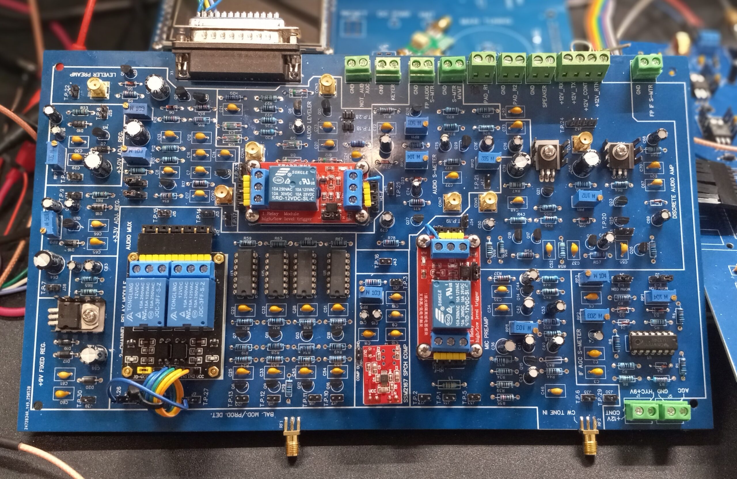 Figure 22. Multifunction Audio Processor Module. This module hosts many audio functions for transmit and receive including, a 4-channel MUX decoder, a 4-channel bidirectional audio MUX, a receive Class AB audio leveler preamplifier, a receive audio leveler/attenuator, a receive Class AB discrete audio amplifier, a receive audio-derived S-meter circuit, a receive IF AGC-derived S-meter circuit, a transmit microphone preamplifier, and a transmit microphone SSM2167 audio compressor.
First Receiver Operation During the WWA Contest
After listening to several stations on the 40 and 20 meter bands, I settled on Portuguese special event station CS2WWA [53] operating on 20 meters during the WWA contest [54] to make a YouTube recording [55] of the receiver audio. From the recovered audio quality, it appears as though the SI5351 BFO frequency has been adjusted properly.
…And a Kuwaiti Station
The next day, I heard a very strong Kuwaiti station, 9K2KO [56], on 20m, . Again, the band was quiet, and the audio was quite good for this YouTube Video [57].
Takeaways
And now, some takeaways from all of this:
· Building this transceiver has turned out to be more of a journey than a destination.
· Homebrew projects are highly rewarding. You really can’t beat the joy that you feel when something that you have built with your own two hands actually works for the first time, and the only way to know how it feels is to experience it for yourself.
· Homebrew projects of this magnitude can be expensive due to printed circuit board fabrication costs with revisions, shipping, tariffs, and minimum component buys. Don’t bite off more than you can chew.
· Homebrew projects need not be complex. They can be as simple as an audio accessory for the shack, or an UNUN for an end fed half wave antenna.
· Seek some mentoring along the way. No one is too old to learn something new. To paraphrase Socrates, “Know what you don’t know.”
· Enjoy some operating time.
References
[1] Blustine, Martin, K1FQL, Spectral Purity of a QRP Transmitter Driver Amplifier, Nashua Area Radio Society, N1FD. May 5, 2026. https://www.n1fd.org/2026/05/05/amplifier-purity/
[2] Scott, Rick, N3FJZ, Circuit6040, Home Page. http://www.remmepark.com/circuit6040/
[3] Scott, Rick, N3FJZ, Circuit6040, YouTube. https://www.youtube.com/@Circuit6040
[4] Carney, Todd, K7TFC, Mostly DIY RF. https://mostlydiyrf.com/
[6] Maiorana, Mike, KU4QO, Kits and Parts, https://kitsandparts.com/IF.php
[7] Blustine, Martin, K1FQL, A Multifunction Audio Processor for SSB Use. Nashua Area Radio Society, N1FD, July 29, 2025. https://www.n1fd.org/2025/07/29/audio-processor/
[8] EasyEDA. https://easyeda.com/
[10] Scott, Rick, N3FJZ, Circuit6040, ZX-SSB-II, Block Diagram. http://www.remmepark.com/circuit6040/ZX-SSB-II/zx_ssb_ii.html#000-AB
[11] Blustine, A Multifunction Audio Processor for SSB Use, op. cit. https://www.n1fd.org/2025/07/29/audio-processor/
[12] Blustine, Martin, K1FQL, A Broadcast Interference (BCI) Notch Filter For General Coverage Receivers, Nashua Area Radio Society, N1FD, November 26, 2024. https://www.n1fd.org/2024/11/26/notch-filter/
[13] Blustine, Martin, K1FQL, Some Fun With Boolean Algebra, Nashua Area Radio Society, N1FD, September 15, 2025. https://www.n1fd.org/2025/09/15/algebra/
[14] Summers, Hans, G0UPL, QRP Labs, https://qrp-labs.com/
[15] Wetherhold, Ed, W3NQN (SK), Second-Harmonic-Optimized Low-Pass Filters, QST, February 1999. https://www.arrl.org/files/file/Technology/tis/info/pdf/9902044.pdf
[16] Digikey Electronics. https://www.digikey.com/?gclsrc=aw.ds&gad_source=1&gad_campaignid=120498675&gclid=CjwKCAjw1IHTBhAaEiwA4AYNFscHyjwzIeu2sGoMkimhWQ5vHmnHuR1RnFixqd3xphUJkEzEp6C2MRoCGa0QAvD_BwE
[18] Maiorana, Mike, KU4QO, Kits and Parts, op. cit.
[19] Magnet Wire, #26 AWG, BNTECHGO, Amazon, https://www.amazon.com/dp/B07DYHHMYH?ref_=ppx_hzsearch_conn_dt_b_fed_asin_title_2&th=1
[20] Wetherhold, Ed, W3NQN (SK), op. cit.
[21] Abhishek Singh, Chintan Patel and Jim Plusquellic, On-Chip Impulse Response Generation for Analog and Mixed-Signal Testing, Proceedings. ITC November 2004. https://ece-research.unm.edu/jimp/pubs/itc2004_abhi.pdf
[22] QORVO, Cascade Analysis Calculator (Active / Passive), https://www.qorvo.com/design-hub/design-tools/interactive/cascade-calculator
[23] Hayward, Wes, W7ZOI, Bob Kopski, K3NHI, A Termination Insensitive Amplifier for Bidirectional Transceivers, June 26, 2009. https://w7zoi.net/bidirectional_matched_amplifier.pdf
[24] Hayward, Wes, W7ZOI, Another Termination Insensitive Amplifier (TIA) Variation, July 19, 2024. https://w7zoi.net/Another_tia.pdf
[25] Summer, Hans, G0UPL, QRP Labs. https://qrp-labs.com/bpfkit.html
[26] Nooelec, Flamingo+ AM – High Attenuation Broadcast AM Bandstop (Notch) Filter v2 https://www.nooelec.com/store/flamingo-plus-am.html?srsltid=AfmBOopje0PGhcnjva_8GofXcZ8cag1bwvQlU9HdRjIL6m49dqaICxB4
[27] Blustine, Martin, Automatic Filter Selection, YouTube Video, July 22, 2026. https://youtu.be/gF3uMe6xbbE
[28] Blustine, Martin, Historical YouTube Record, First CW Reception Using the SI5351 Synthesizer To Generate LO and BFO Frequencies, April 14, 2024. https://youtu.be/kqMMev3dB7Y
[29] Blustine, Martin, Historical YouTube Record, First SSB Reception Using the SI5351 Synthesizer To Generate LO and BFO Frequencies, April 14, 2024. https://youtu.be/MyEZmxg1DTQ
[30] Blustine, Martin, K1FQL, An RF to IF Converter for QRP SSB Transceiver Use, Nashua Amateur Radio Society, N1FD, August 4, 2025. https://www.n1fd.org/2025/08/04/transverter/
[31] Carney, Todd, K7TFC, Mostly DIY RF. https://mostlydiyrf.com/tia-agc/
[32] CalOutlet, eBay, Connectorized Mini Circuits ADE-1 Mixer, https://www.ebay.com/itm/134905816984?_skw=ADE-1+Mixer&itmmeta=01KY6CDSRPBNFBZWXH0NT2ZNM7&hash=item1f69036798:g:9lgAAOSwggFlsekp&itmprp=enc%3AAQALAAAA8GfYFPkwiKCW4ZNSs2u11xBTxJihuaEwUic%2BP1s46fXrS1M5n6EpBYsw42848FpEqB75aT8Gqskzjl%2BgqAldfOWDv80ckkjKYtgDQyyVd42UFD2y1NcsgO9YOComyrJh5LJSxL%2FGEsoMnBRL7kmIXQwVmn5q75r8QvrK8dRZLoiycWWDI2wATK1jSqpW3JL%2BuElHP00vIW61Ghd1Ykst%2FYbigtAhgY3FMxrkwK1S4%2BvO6qjNAN0sTuH5xjUqLaV77%2BrmJ2PmFi5GyRwiDB6PtlCNyNZw0UpzrZgypy6%2FDfRgaBzz1nFKZUJs%2Bfjbfyg2Pw%3D%3D%7Ctkp%3ABk9SR9Kct8zxZw
[33] Adafruit Si5351A Clock Generator Breakout Board – 8KHz to 160MHz, https://www.adafruit.com/product/2045?srsltid=AfmBOooUwpLmUUGk3frLK4TMJqUfOkExu4rlJZINbsIml1ROuhN0ilzk
[34] land-boards.com, https://land-boards.com/blwiki/index.php?title=A_Termination_Insensitive_Amplifier_for_Bidirectional_Transceivers
[35] Blustine, Martin, A Switchable Crystal Filter Module for SSB and CW, Nashua Area Radio Society, N1FD, TBA.
[36] Carney, Todd, K7TFC, Mostly DIY RF, 8-Pole QER Crystal Filters, https://mostlydiyrf.com/qer/
[37] Blustine, Martin, K1FQL, IF to Audio Baseband Converters for QRP SSB, Nashua Area Radio Society, N1FD, August 21, 2025. https://www.n1fd.org/2025/08/21/audio-converters/
[38] land-boards.com, op. cit.
[39] Connectorized Mini Circuits ADE-1 Mixer, CalOutlet, eBay, op. cit.
[40] Lewallen, Roy, W7EL, An Optimized QRP Transceiver for 7 MHz, QST, August 1980, pp. 14-19. https://www.worldradiohistory.com/Archive-DX/QST/80s/QST-1980-08.pdf
[41] Adafruit Si5351A Clock Generator Breakout Board, op. cit.
[42] Scott, Rick, N3FJZ, Audio Amp with TX Mute, http://www.remmepark.com/circuit6040/MAX-SSB/images/MAX-SSB_(150)_Audio_Amp_w_TX_Mute.png
[43] Scott, Rick, N3FJZ, Power Management MOSFET Switching. http://www.remmepark.com/circuit6040/ZX-SSB-II/images/(100)_ZX-SSB-II_Power_man_MOSFET.png
[44] Blustine, Martin, K1FQL, A 4-Channel Audio Multiplexer That You Can Build, Nashua Area Radio Society, N1FD, June 9. 2025. https://www.n1fd.org/2025/06/09/audio-multiplexer/
[45] Ibid.
[46] Andersen, Rick, KE3IJ (SK), General Purpose Audio Amplifier. https://mostlydiyrf.com/gpaa/
[47] Wolke, Alan, W2AEW, #157: Circuit fun: Automatic audio leveling circuit | audio compressor | for scanning receiver, YouTube, https://www.youtube.com/watch?v=1h0FZJYXQ_w
[48] Scott, Rick, N3FJZ, Audio Amp with TX Mute, http://www.remmepark.com/circuit6040/MAX-SSB/images/MAX-SSB_(150)_Audio_Amp_w_TX_Mute.png
[49] Scott, Rick, N3FJZ, S-Meter, http://www.remmepark.com/circuit6040/ZX-SSB-II/images/(130)_ZX-SSB-II_S-Meter.png
[50] Hayward, Wes, W7ZOI, S-Meter Driver for Hybrid Cascode IF Amplifier, https://w7zoi.net/hycas-apps.html
[51] Morris, Charlie, ZL2CTM, Homebrew 80m/40m SSB/CW Rig – Part 3: Mic Amplifier, YouTube. https://www.youtube.com/watch?v=uX0ptaHokFI&t=527s
[52] Analog Devices, SSM2167 Low Voltage Microphone Preamplifier with Variable Compression & Noise Gating. https://www.analog.com/media/en/technical-documentation/data-sheets/SSM2167.pdf
[53] CS2WWA, Portugal, WWA 2026 Sprint Station, https://www.qrz.com/db/CS2WWA
[54] Worldwide Award (WWA) Sprint Webpage, https://hamaward.cloud/wwa
[55] CS2WWA, YouTube Recording https://youtu.be/FTIwe8hzqSM
[56] 9K2KO, Kuwait, https://www.qrz.com/db/9K2KO
[57] 9K2KO, YouTube Recording https://youtu.be/GrckfTXeARI
Disclaimer
This circuit design is provided for informational and educational purposes only and is supplied “as is” and without warranties of any kind, express, implied, or statutory. No representations or warranties are made regarding the accuracy, adequacy, completeness, legality, reliability, or usefulness of this information, either in isolation or in the aggregate. This circuit design may contain links to or information based on external sources or third-party content. Endorsement and responsibility for the accuracy or reliability of such third-party information or for the content of any linked websites are not taken.

_Audio_Amp_w_TX_Mute.png)
_ZX-SSB-II_Power_man_MOSFET.png)
_ZX-SSB-II_S-Meter.png)