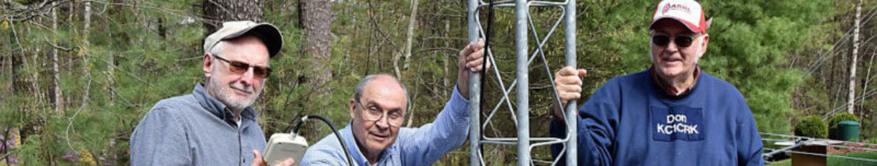
It’s that time again, and Winter Field Day will be here before you know it. Planning is well underway. Once again, Fred and Anita have opened their home and shack for Winter Field Day operation, and we will be operating QRP (10 Watts or less), which is a score multiplier. This year a new multiplier category was added to operate on an additional six (6) bands to make it a total of twelve (12) bands.
This past weekend, Fred, AB1OC, and I tested six additional bands with overwhelming success from his QTH to a mobile location I operated, acting as the roving team. They say sharing is caring, so I thought I would write a blog about how we got here and the tools that helped along the way.
Winter Field Day Rules
All the rules are available here; the three specific ones to note are as follows.
Bands: All Amateur bands may be used except 12, 17, 30, and 60 meters. To qualify as a band worked, at least one valid, two-way QSO must have taken place on the said band during the event.
Make three contacts on at least six (6) different bands: Conditions may change throughout an event. Log operations on at least six different bands by making a minimum of three contacts per band. You should be able to accomplish this objective by utilizing HF, VHF, and UHF frequencies. Don’t forget about 1.25 meters (220)! It’s an excellent band for local emergencies. OM x6
Make three contacts on at least twelve (12) different bands: Was six too easy? You may have to pull out your microwave equipment to achieve this one. Log operations on at least twelve different bands by making a minimum of three contacts per band. The six bands from the previous objective count toward this one. OM x6
The first 6 bands are the typical contesting bands: 10m, 15m, 20m, 40m, 80m, 160m. No problem for the AB1OC shack. The other 6 bands will be 6M, 2M, 1.25M, 70CM, 33cm, and 23cm. Here are the challenges.
1) We can’t use a repeater. Simplex only.
2) Since it is VHF and UHF, we need a decent Line of Sight (LOS) with little or no trees to cause interference.
3) We are running QRP, so distance is a factor.
4) We need equipment for the 33cm and 23cm bands.
5) We need at least three contacts.
VHF/UHF Roving
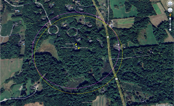
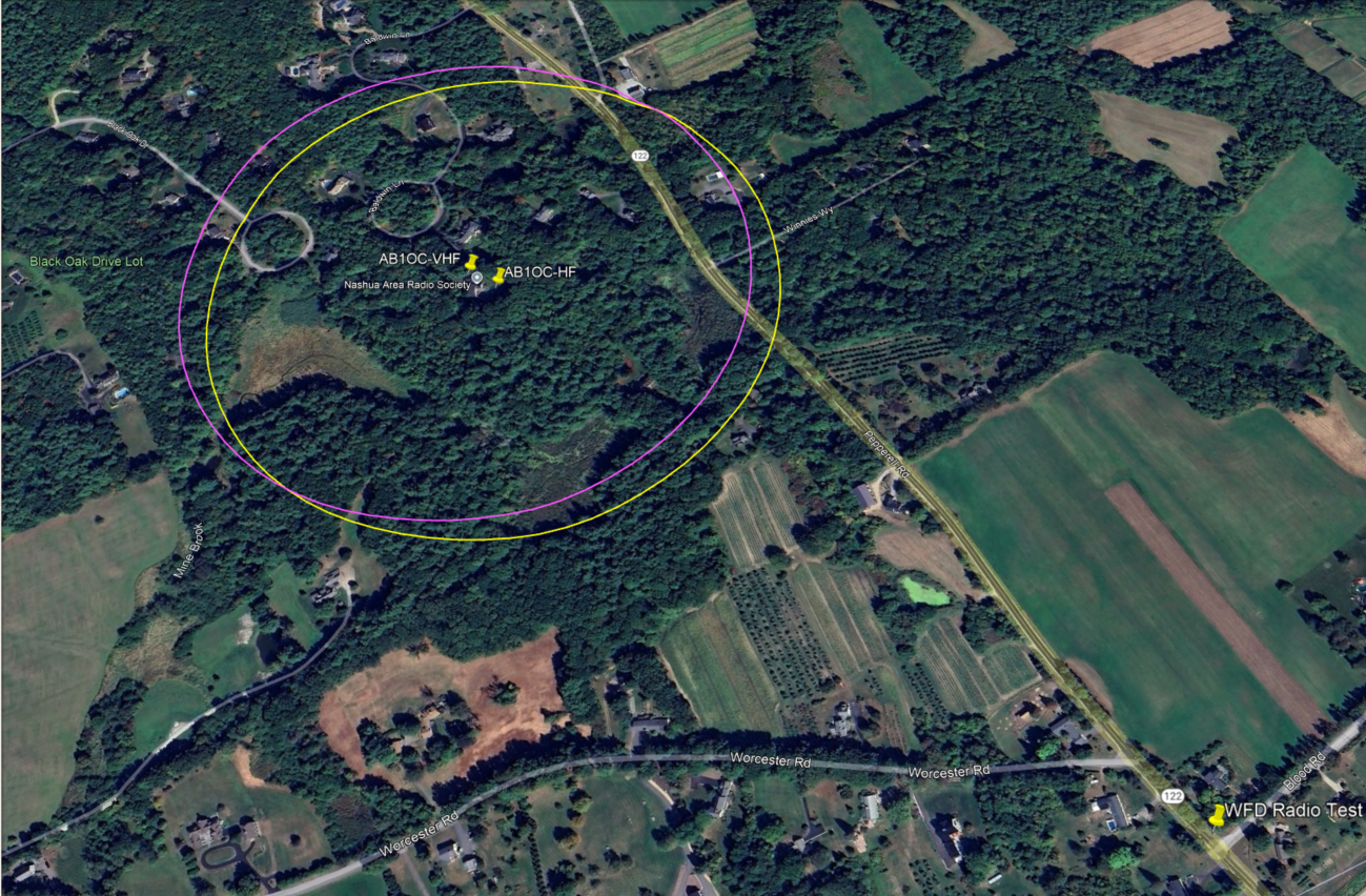
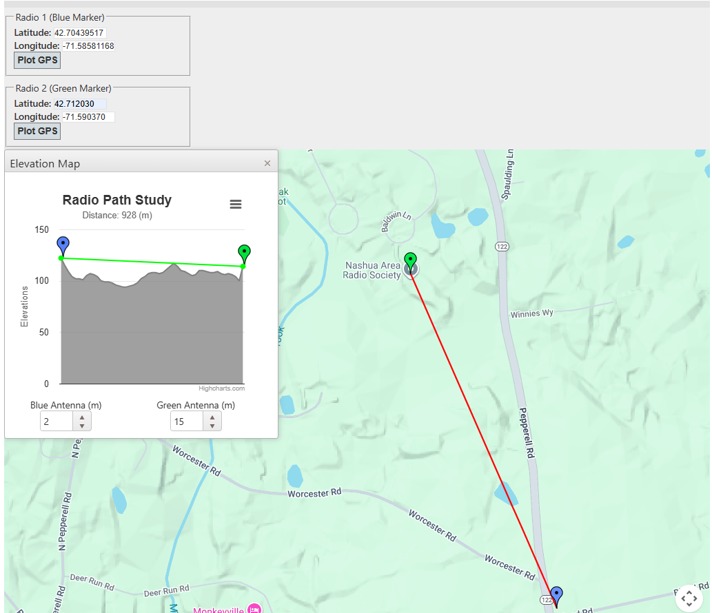
As part of the planning and to address these problems, we decided to send a Roving team to serve as the club’s three contacts. Rules dictate that contacts must be outside a 1000 ft circle from the Field Day base of operation. I started by using Google Earth Pro, setting the coordinates for AB1OC QTH and using the circle ruler to determine our 1000-foot perimeter. The two circles represent the VFH and HF Towers’ location.
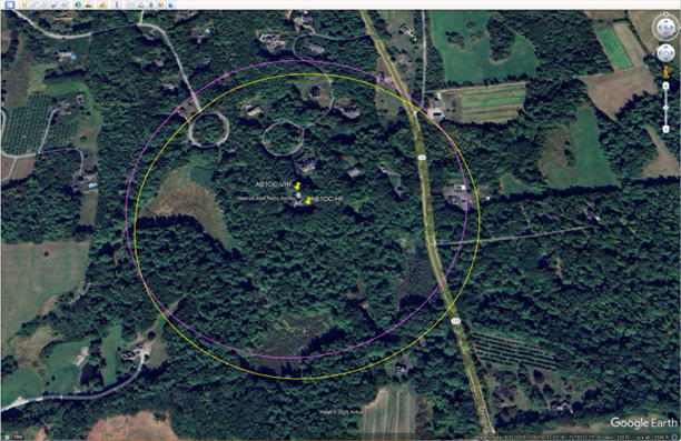
Based on the knowledge of the surrounding area, we chose the location southeast of the intersection of RT 122 and Blood Road.
Then we used the HeyWhatsThat website to generate ideas for where we could get a signal based on the topology.
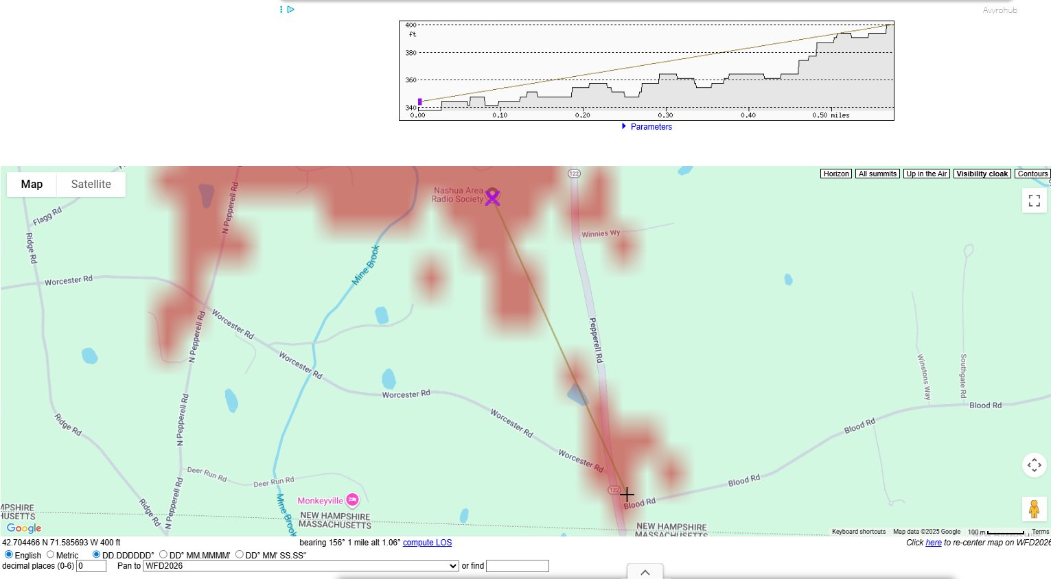
And the Scadacore LOS website to confirm the topology.
Both are very simple to use.
We looked at a few other locations, but tested this site first and had great success, so we called it a win for Winter Field Day.
Another interesting tool is Radio Mobile. This software is a popular, free radio propagation simulation software for planning wireless networks (especially for amateur radio).
They offer both web and download versions. The download version has more features and is worth a peek. This YouTube video is a great tutorial that walks you through installing your first propagation map. Could be a Tech Night session!
I started loading all the variables, but since our field test was successful, I didn’t complete the simulation.
Rover Radios and Antennas
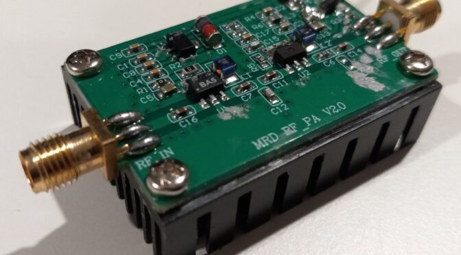
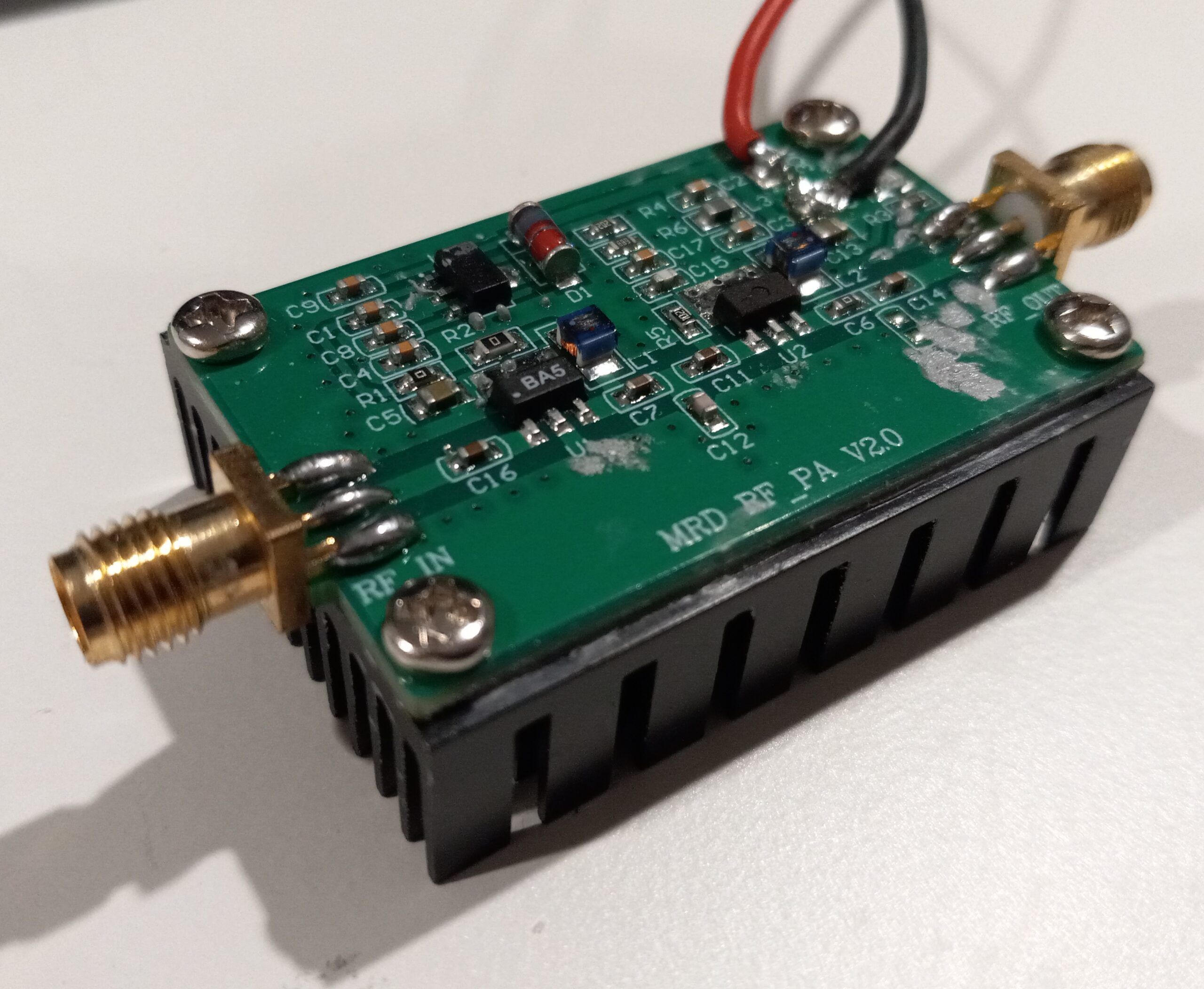
For equipment, Fred’s SDR can handle all the required bands, and his antennas are up to the task.
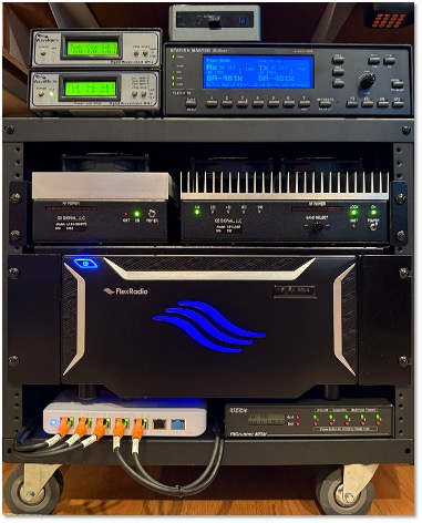
Here is what we are working with for antennas at the base station:
- 6m Loop Yagi (14.1 dBi)
- 1.25m Yagi (11.9 dBi)
- 2m Circularly Polarized Yagi (14.4 dBic)
- 70cm Circularly Polarized Yagi (18.9 dBic)
- 33cm Yagi (15.2 dBi)
- 23cm Yagi (17 dBi)
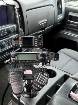
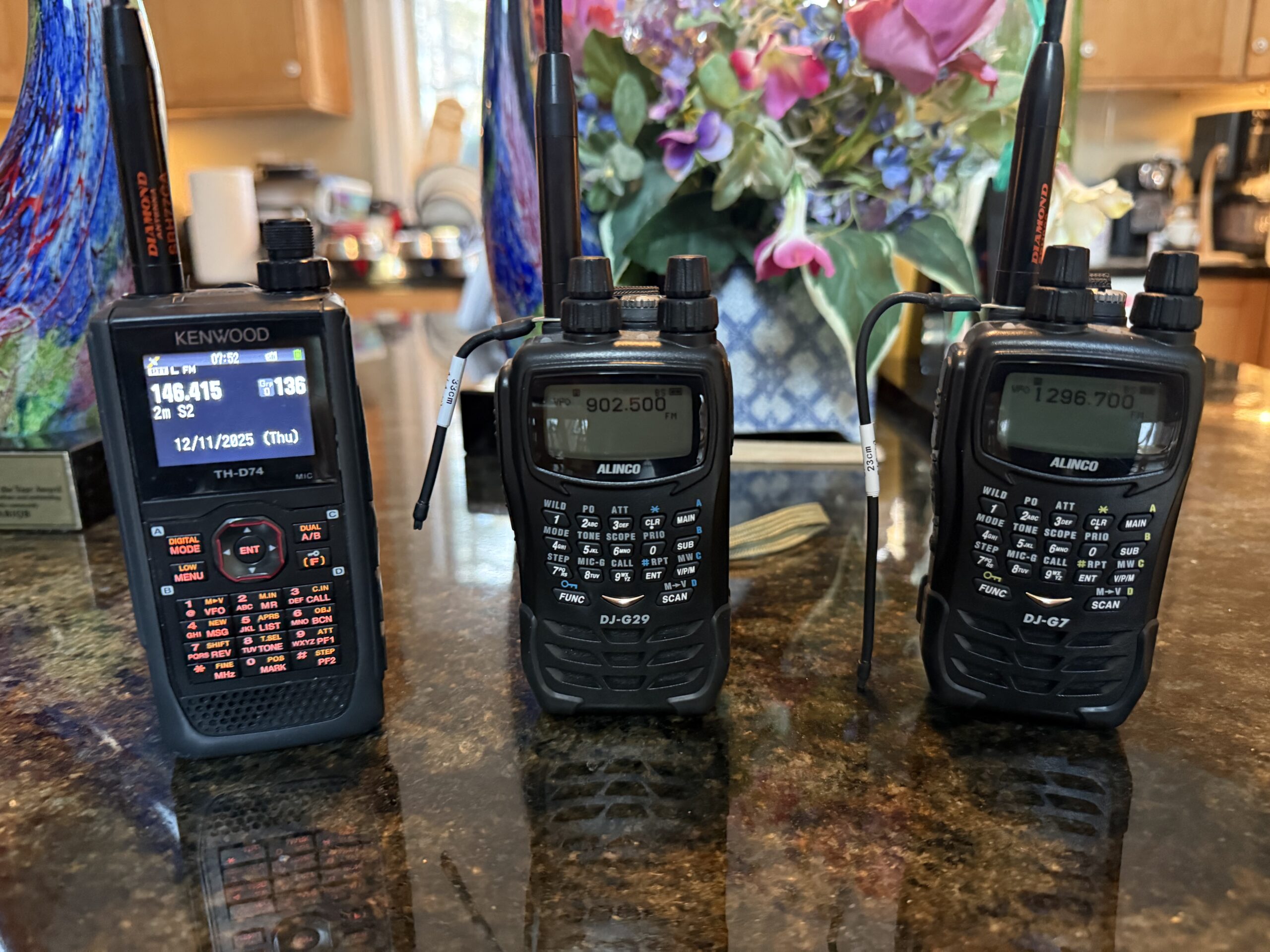
Even at the QRP level, the gain and ability to point the antennas helped overcome distance issues. For the roving team location, I used a 33 cm Alinco HT with a short radial, a 23 cm Alinco HT also with a short radial, a Kenwood HT for 2M, 70cm, and 1.25m from Fred’s stash—finally, a Yaesu 891 with ATAS 120 Antenna for 6M as part of my mobile rig.
Specifically, we tested the following:
2M 146.415 MHz Vertically Polarized
1.25M 223.500 MHz Horizontally Polarized
70CM 445.925 MHz Vertically Polarized
33cm 902.500 MHz Horizontally Polarized
23cm 1296.700 MHz Horizontally Polarized.
6M 50.150 MHz SSB Horizontally Polarized
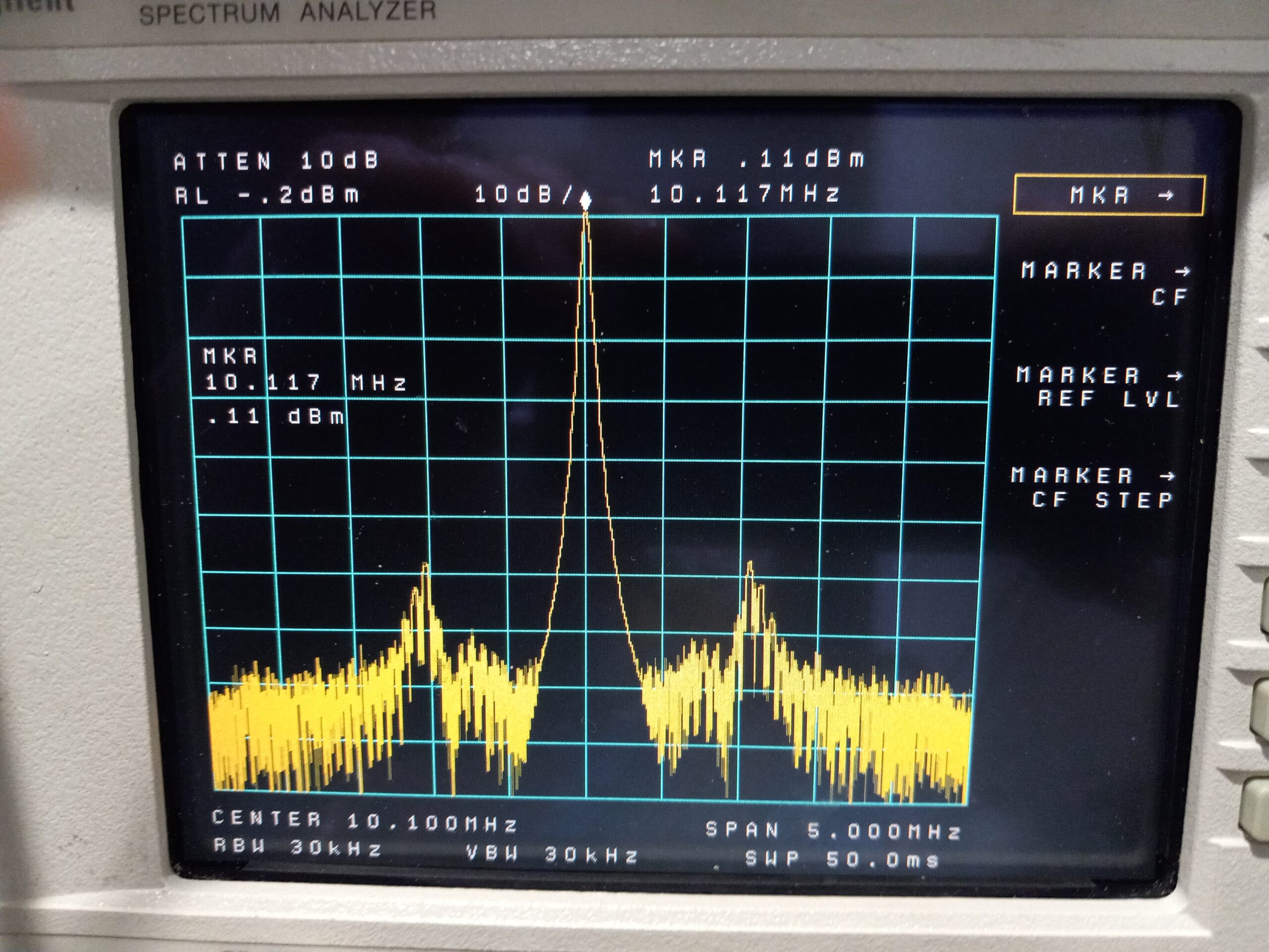
As we cycled through the bands and our QSO, the signal reports were between 57 and 59 at both ends. Our 5 challenges were easily overcome.
With a month to go before Winter Field Day, we are ready and excited to have fun, learn, and earn points. We are still looking for volunteer rovers, which is an excellent opportunity for Techs. Don’t worry if you’re new; you will have help. If you are interested in participating in any part of Winter Field Day or in planning, please contact us or join the planning meeting.
Dave, K1BER