The Nashua Area Radio Society (N1FD) successfully completed Winter Field Day 2026, operating on January 24–25 under some of the harshest winter conditions we’ve experienced in recent years. Bitter cold persisted throughout the weekend, followed by a snowstorm on Sunday afternoon, yet the club achieved all planned multipliers and delivered a strong overall result.
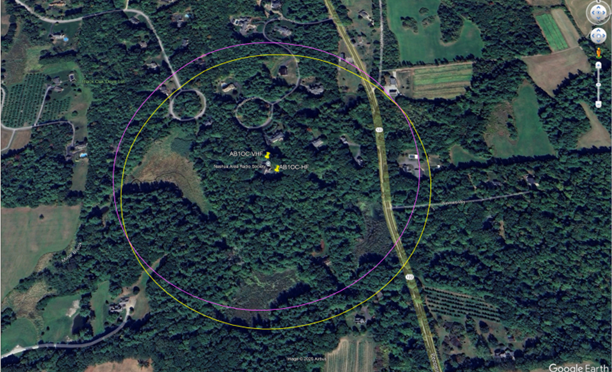
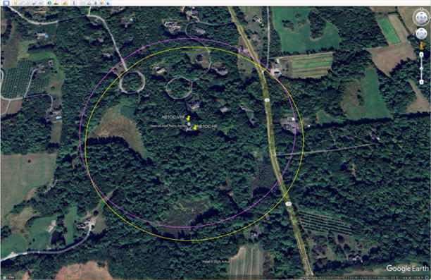
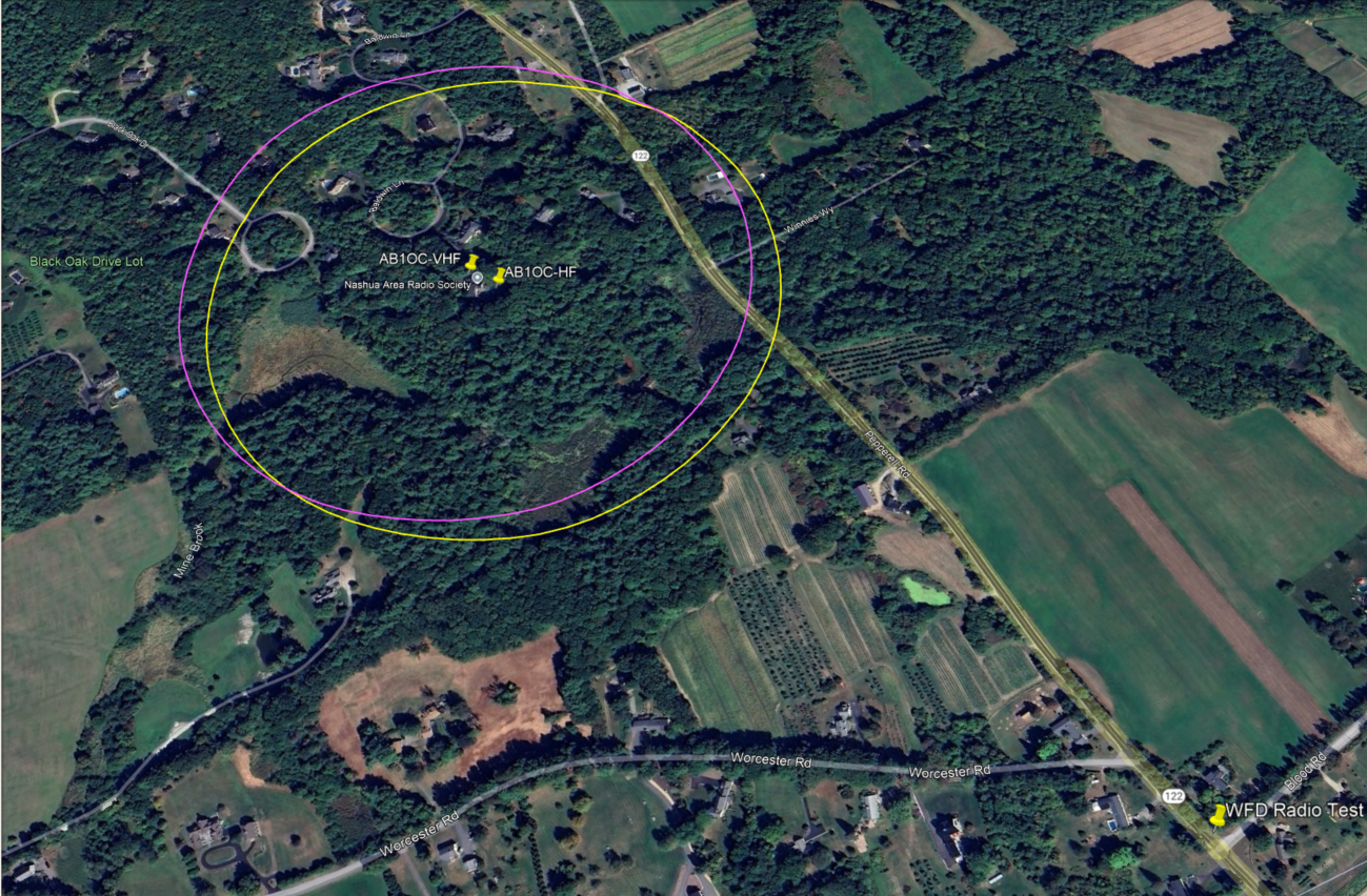
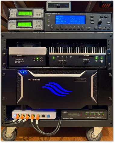
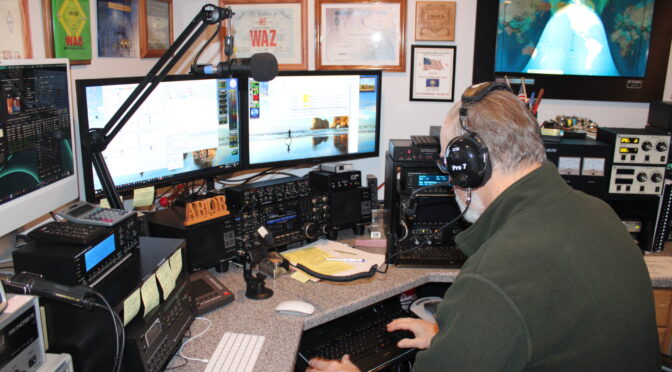
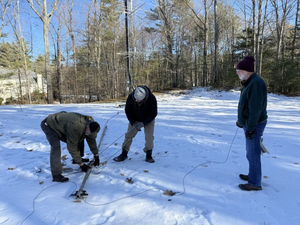
N1FD operated as Class 2H, with all stations located indoors at the QTH of Fred Kemmerer, AB1OC, and Anita Kemmerer, AB1QB. Antennas were deployed outdoors, allowing operators to remain warm, safe, and focused while fully meeting the operating and technical challenges of Winter Field Day.
Preparation Made the Difference
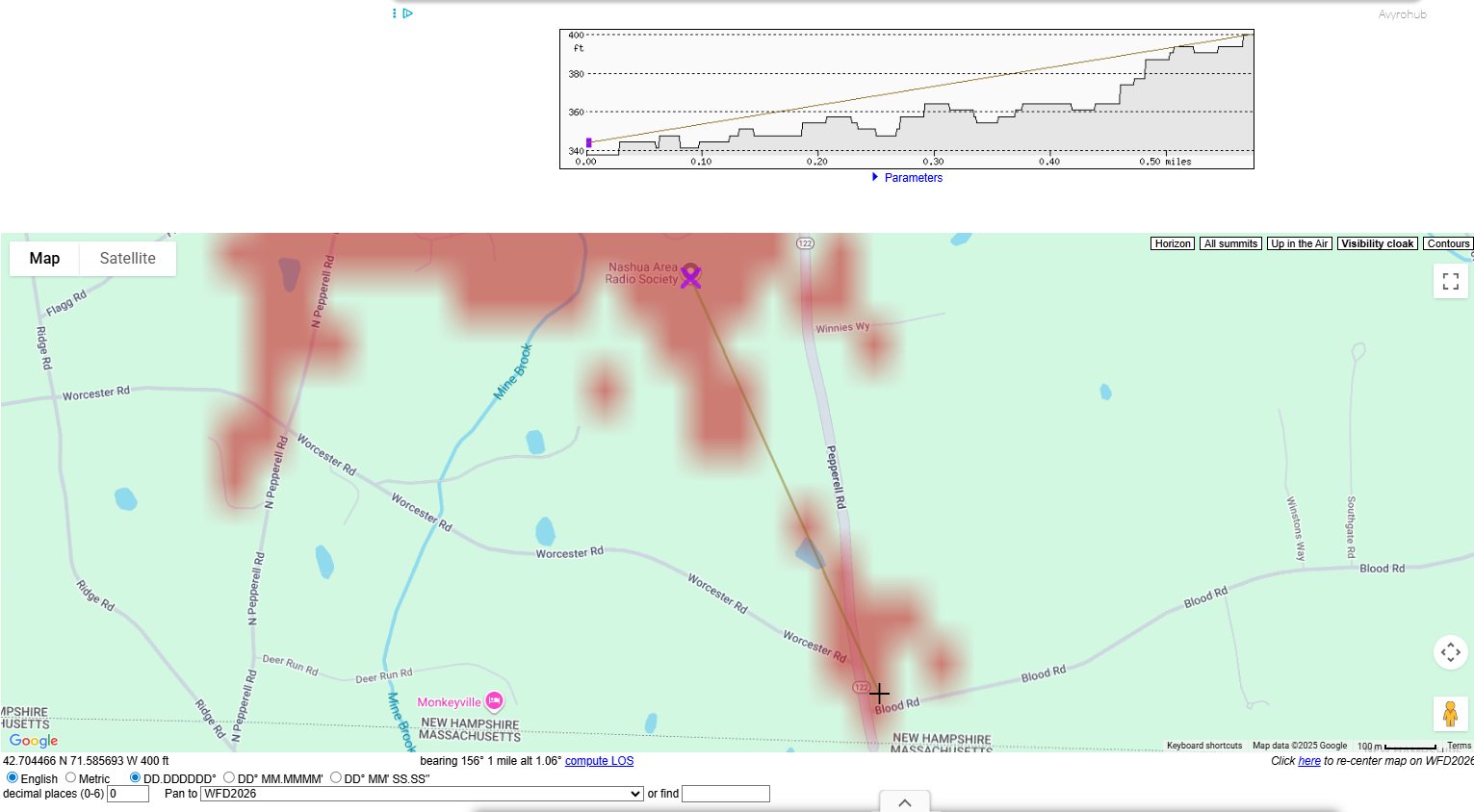
Winter Field Day success was the result of careful planning and coordination in the weeks leading up to the event. The club focused on targeting specific band and mode multipliers, ensuring coverage across HF, VHF, and UHF, coordinating operator schedules and operating strategies, and verifying station readiness and antenna performance.
That preparation paid off, allowing N1FD to methodically work bands and modes and complete every planned multiplier without last-minute pressure.
QSO and Band Results
During the weekend, N1FD logged:
| Band | Mode | QSOs | Pts |
|---|---|---|---|
| 160 m | CW | 55 | 110 |
| 80 m | LSB | 20 | 20 |
| 40 m | LSB | 81 | 81 |
| 20 m | PSK31 | 1 | 2 |
| 20 m | USB | 445 | 445 |
| 15 m | USB | 337 | 337 |
| 10 m | USB | 81 | 81 |
| 6 m | USB | 3 | 3 |
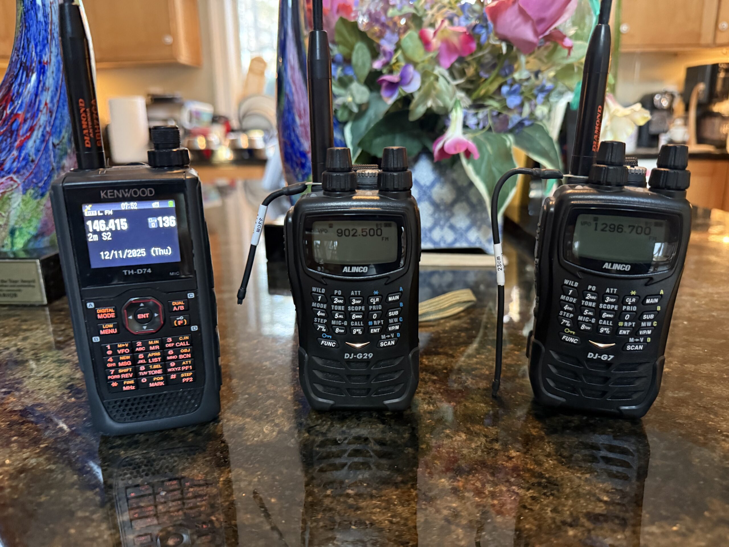
| 2 m | FM | 3 | 3 |
| 1.2 m | FM | 3 | 3 |
| 70 cm | FM | 3 | 3 |
| 33 cm | FM | 3 | 3 |
| 23 cm | FM | 3 | 3 |
| Total | All | 1038 | 1094 |
1,038 total QSOs
1,094 total QSO points
28 total multipliers
Based on these results, N1FD’s estimated final score was:
1,094 QSO points × 28 multipliers = 31,726 points
The strongest activity came from 20 meters (USB) and 15 meters (USB), with solid participation across 40 meters, 80 meters (CW), digital modes, and successful contacts on VHF and UHF, all of which were critical to completing the multiplier plan.
Multipliers Achieved
A major objective for Winter Field Day 2026 was to intentionally pursue as many multipliers as possible through planning and disciplined operating. N1FD successfully completed every multiplier we set out to achieve, resulting in a total multiplier of 29X, including the 1X multiplier added for participation.
The following multipliers were earned during the event.
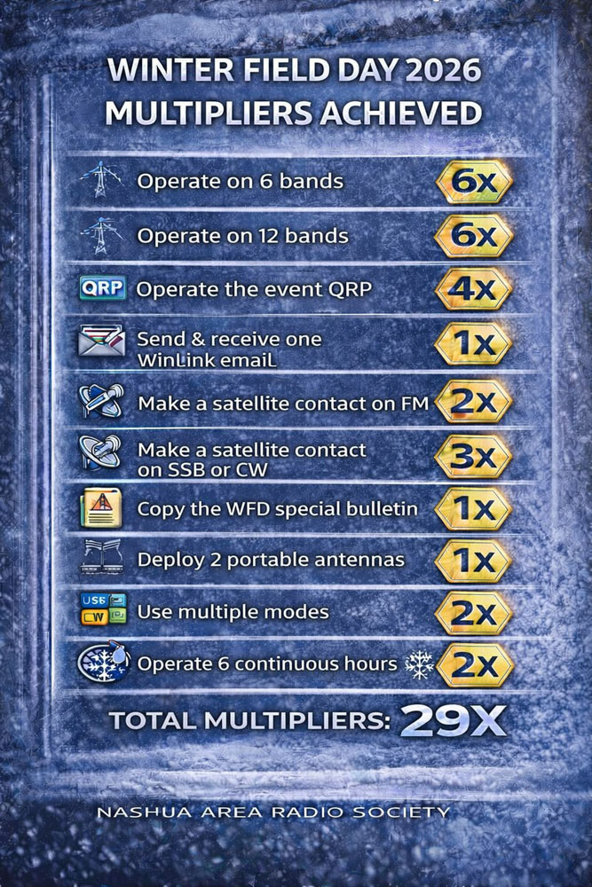
Completing the full multiplier set was a direct result of advance planning, operator coordination, and flexibility throughout the weekend.
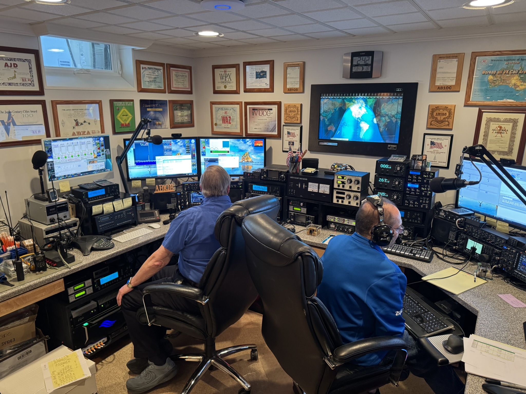
Operators on the Air
The following members operated under the N1FD callsign during Winter Field Day:
- Alan Whitney, KC1PWB
- Fred Kemmerer, AB1OC
- Brian Quick, W1XMM
- Joe Luszcz, AC1LN
- Anthony Rizzolo, KC1DXL
- Dave Cherkus, N1AI
- Mike Swatko, W1TKO
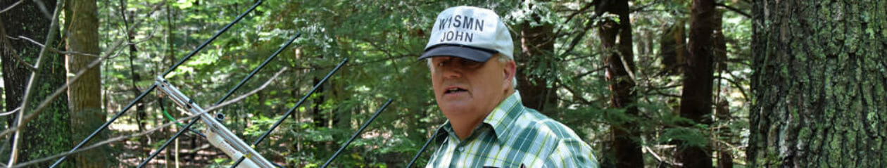
- John Halbert, W1SMN
- Anita Kemmerer, AB1QB
Operators rotated across bands and modes to keep stations active and productive throughout the event.
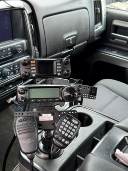
VHF Rover Participation
In addition to the fixed indoor stations, three N1FD members participated as VHF Rovers, helping us to achieve the 12-band multiplier.
Their rover operations added an important mobile element to N1FD’s Winter Field Day effort.
Special Thanks
Special thanks go to Joe Luszcz, AC1LN, and Brian Quick, W1XMM, who installed the wire antennas on Friday, January 23rd, working outdoors in very cold weather to ensure the stations were fully operational before the event began.
Additional recognition goes to Fred Kemmerer, AB1OC, who spent many long hours preparing the station, testing equipment, and resolving technical details ahead of Winter Field Day. His dedication was critical to the smooth operation and success of the weekend.
We would also like to thank Brian Quick, W1XMM, for his leadership in planning and coordinating Winter Field Day 2026 in his role as Field Day Chairman. His organization and preparation were instrumental in helping the club meet its operating and multiplier goals.
Special thanks to Dave Cherkus, N1AI, for operating 160-meter CW, helping N1FD make effective use of the low bands during challenging winter conditions.
Thank you to Dave Berardinelli, K1BER, for leading and coordinating the VHF Rover effort, which played an important role in expanding our band coverage and multiplier success.
Finally, thank you to all of the operators who participated throughout the weekend. Your time, flexibility, and teamwork made this Winter Field Day a success.
A Successful Winter Operation
Winter Field Day 2026 once again demonstrated what N1FD does best: strong planning, teamwork, and adaptability, even under challenging winter conditions. Operating indoors allowed the club to stay safe and effective while still delivering excellent on-air results.
Thank you to everyone who planned, set up, operated, and supported this effort. We look forward to building on this success for future Field Days and operating events.