I haven’t had the occasion to use any programming languages since retirement. That’s why the addition of a Raspberry Pi 4 Model B to the shack was a welcome change. I like to think of the Raspberry Pi as just another computer – one that uses a different operating system. With the Raspberry Pi, I can browse the Internet, access email, and write and run programs.
When I began to assemble a shack, I reserved a space on the wall for a 32″ TV, Figure 1, which was purchased during a temporary rental stay. That TV has been unused for 3 years, but it was earmarked for a HamClock.
 Figure 1. Unused 32″ TV Earmarked for HamClock. The TV was wall-mounted above the shack monitors. Please click on image to expand.
I searched the N1FD site to see if anyone had written about HamClock, but no articles were found. The first article for HamClock, written by Elwood Downey, WB0OEW, appeared in October 2017 QST[1]. In his article, he calls for the use of an Adafruit HUZZAH ESP8266 Wi-Fi system-on-chip. That device was fastened to the back of a 7″ TFT display.
The version of HamClock that I built for use with the 32″ HDTV employs the Raspberry Pi 4 Model B, Figure 2, with 2 GB memory[2]. The kit that I found on Amazon includes a 64 GB microSD card (with USB adapter) onto which the Raspberry Pi operating system had been preloaded. The kit also includes a plastic case with fan, little rubber feet, tiny screws to attach a camera, device heatsinks, a wall-wart power supply, a micro HDMI to HDMI cable, an instruction manual and various assembly instruction cards. The user has to provide their own USB mouse and keyboard. I already owned a wireless mouse and keyboard so I was able to use a single USB 2.0 port on the Pi for the wireless adapter.
If you already have a microSD memory card with USB adapter, power supply, mouse, keyboard and HDMI cable, you could get by with a Raspberry Pi Zero[3] at one-fourth the price.
 Figure 2. Raspberry Pi 4 With Wireless Mouse and Keyboard. A single USB 2.0 port on the Pi is used for the wireless adapter leaving 1 x USB 2.0 and 2 x USB 3.0 ports unused. Power and HDMI cables are visible. Please click on image to expand.
If your Raspberry Pi does not come equipped with the operating system installed, you can download it from the official Raspberry Pi website and store it on a microSD card for installation provided that you have a USB to microSD card adapter. The Raspberry Pi site allows you to select an operating system and it allows you to specify where the operating system will be stored upon download:
https://www.raspberrypi.com/software/
Please, follow the directions to install the operating system on your device.
I noticed an ambiguity in the kit documentation regarding connection of the cooling fan to the Pi bus header. A tiny drawing, Figure 3, shows where the red and black leads should be connected, namely pins 1 and 14, respectively. The documentation should make it clear that the long header row that contains pin 1 contains all of the odd-numbered pins while the long header row that contains pin 14 contains all of the even-numbered pins. This makes it a bit easier to locate pin 14. Figure 3. Location of the Fan Voltage Pins. The long header row that contains pin 1 contains all of the odd-numbered pins while the long header row that contains pin 14 contains all of the even-numbered pins. Please click on image to expand.
The instructions advise that the HDMI port closest to the DC power supply input be employed if only one monitor will be used. I was confused about the power supply connector. It may be plugged into the Pi upside down. However, I found that a bright flashlight can be used to look inside the power supply connector and inside the Pi power supply input jack to ensure that the conductive contacts face one another. If the connector has been plugged in correctly, some LED status lights on the Pi circuit card should illuminate once the inline DC power cord switch, Figure 4, has been turned on.
This switch has to be used with caution. The operating system, if running, must be shut down prior to turning the DC power switch to the off position. Failure to do so could corrupt data stored in memory and on the microSD card. This is a minor weakness in the design.
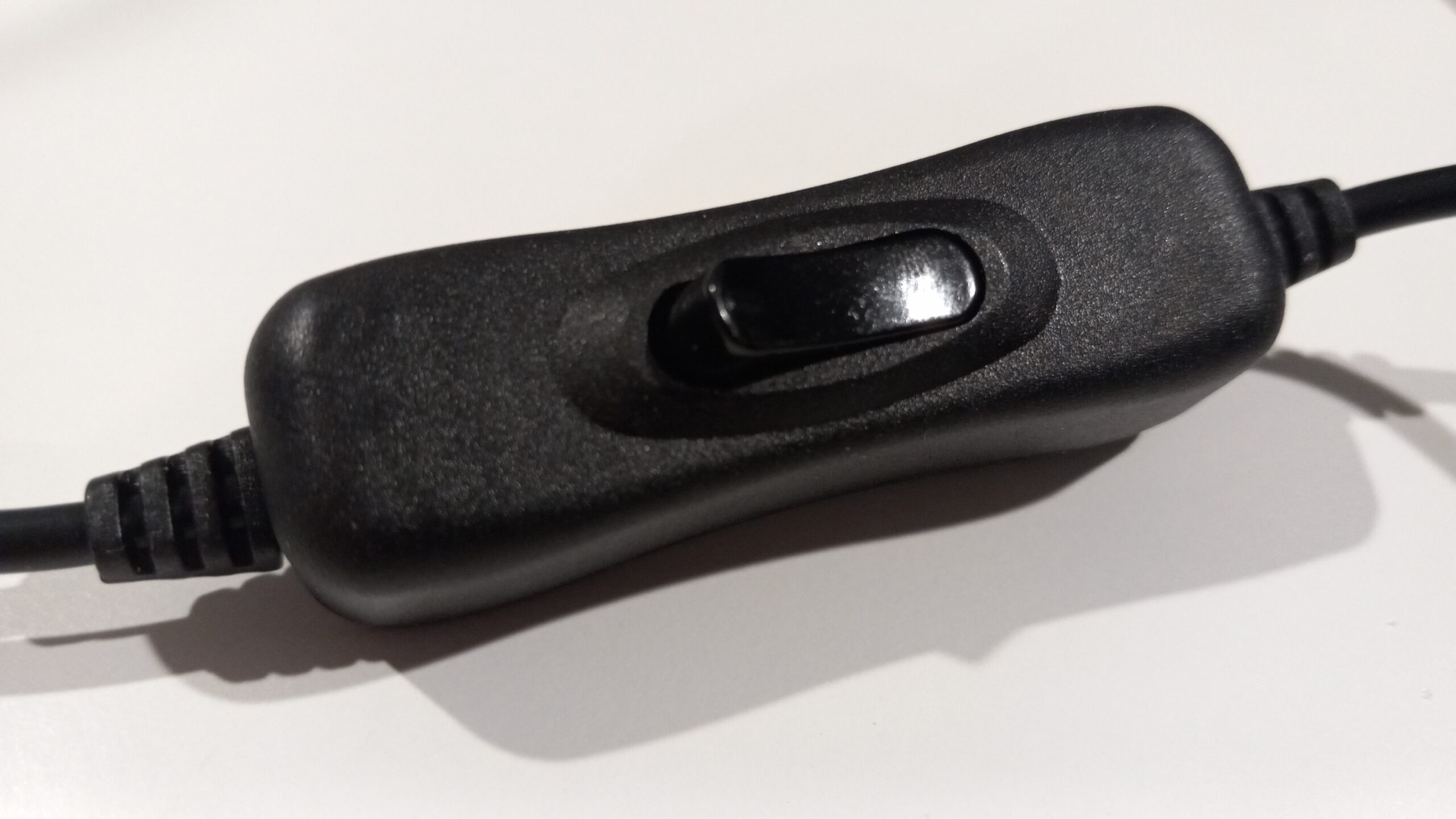 Figure 4. The Inline DC Power Switch. The operating system must be shut down from the Raspberry Pi menu icon on the taskbar before turning the DC power switch to the off position. Please click on image to expand.
Two methods may be used to shut down the Raspberry Pi. There is a Raspberry icon that appears on the taskbar. One of the drop-down selections is to log out. Once selected, another dropdown appears that offers the choice to shutdown or reboot. There is a second method that permits shutdown from a terminal window, Figure 5, which may be opened from the taskbar. One need only enter the command:
sudo shutdown -h now
to close the operating system. A third option is to add a momentary switch to the Pi bus header. That may be used to assert a shutdown command for the operating system. I have not implemented that feature.
 Figure 5. Terminal Window. A terminal window may be opened from the Pi taskbar. Please click on image to expand.
Once an unused HDMI input to the monitor or TV is selected, and the mouse, keyboard and HDMI cable are plugged in, the power switch in the supply power cord may be switched on. Within seconds the Raspberry Pi logo appears followed by a series of questions that include language and time zone. The operating system will also ask for access to WiFi. I found that WiFi was easier than connecting another Ethernet cable to the access point.
Once WiFi is connected, the operating system will update. Finally, a desktop appears. The taskbar was docked to the top of the screen, but I moved it to the bottom because that is where I am used to seeing it, Figure 6. That may be accomplished by selecting that feature from the Raspberry Pi icon on the taskbar. The operating system provides access to the Internet via a browser icon that appears on the taskbar. There are also icons for a terminal window and Bluetooth.
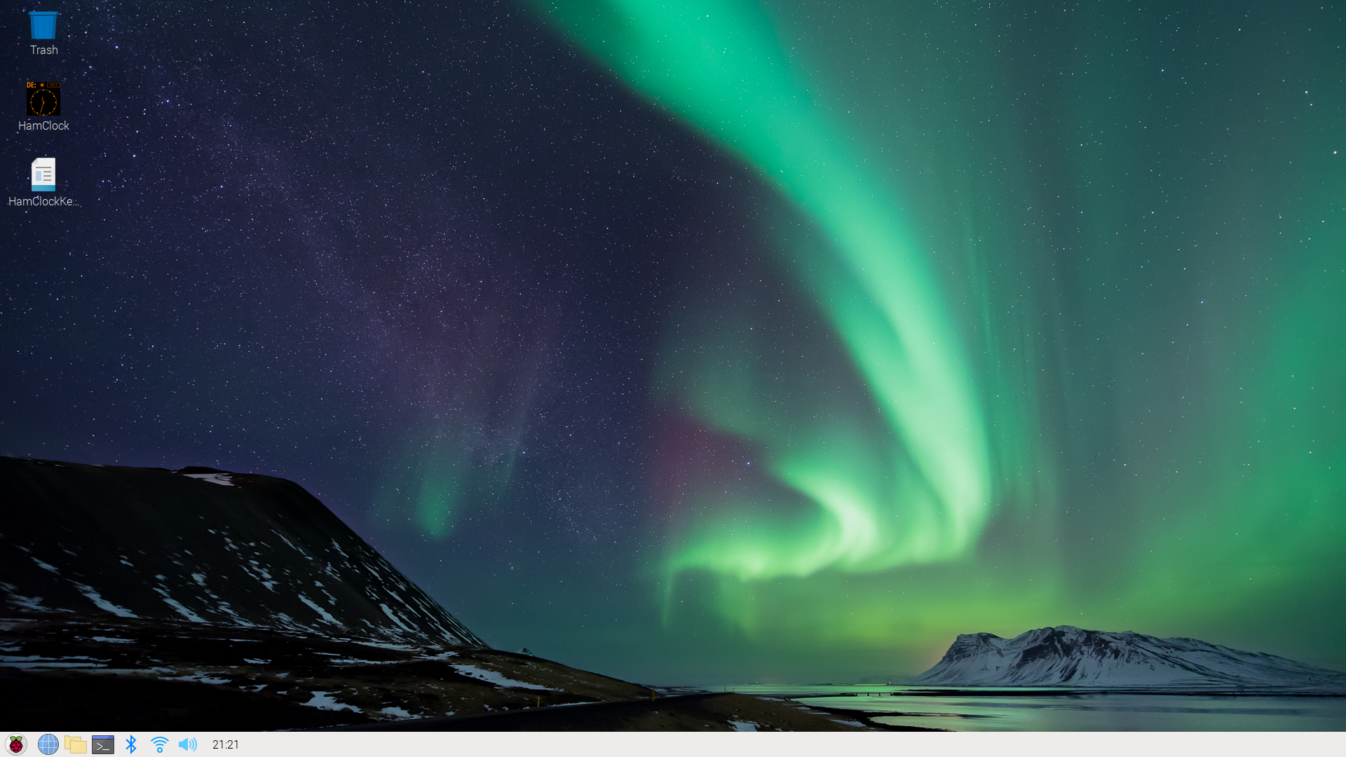 Figure 6. Taskbar Moved and Docked to the Bottom of the Screen. This may be selected from screen appearance under the Raspberry Pi icon on the taskbar. Wallpaper like this may be selected from a list. Please click on image to expand.
The Raspberry Pi icon, Figure 7, provides several selections for screen appearance, resolution and the usual accessories. It also provides a means for shutting down the operating system.
 Figure 7. Menu Provided Under Raspberry Pi Accessible from Taskbar. Access to many options is provided here including Raspberry Pi screen resolution. This is not the same as the HamClock screen resolution setting, which will be selected separately. Please click on image to expand.
It was learned that the means for capturing screenshots within the Pi operating system is Print Screen (PrtSc) just as it is in Windows, so this method has been used to illustrate this article. The images are stored as PNG files in the home Raspberry Pi folder, not under Screenshots in the Photo folder where one would expect them to be.
After opening a terminal window, I followed the directions provided at the Clear Sky Institute[4] web page under the Desktop tab with some notable exceptions. First, I took the advice of KM4ACK[5] to circumvent error messages by executing two scripts before attempting anything else. These scripts may be found listed under the Desktop tab under the subsection titled “To install HamClock on other UNIX-like systems follow these steps”, paragraph 2, “If you get errors”[6]. These steps at Clear Sky are correct except for a syntax error pointed out by KM4ACK[7] in the script:
sudo apt-get -y curl install make g++ libx11-dev xserver-xorg raspberrypi-ui-mods libraspberrypi-dev linux-libc-dev lightdm lxsession openssl
This script must be corrected so that the word ‘install’ precedes the word “curl”. The corrected script should read:
sudo apt-get -y install curl make g++ libx11-dev xserver-xorg raspberrypi-ui-mods libraspberrypi-dev linux-libc-dev lightdm lxsession openssl
I don’t know why this has not been corrected on the Clear Sky Institute web page, but I am happy that KM4ACK pointed it out.
We may now follow the steps listed under “To install HamClock on a Raspberry Pi follow these steps”. It is suggested that the lines of code be executed line-by-line.
cd
curl -O http://www.clearskyinstitute.com/ham/HamClock/install-hc-rpi
chmod u+x install-hc-rpi
./install-hc-rpi
If you choose not to install a desktop icon, you may run this script from a terminal window to start HamClock:
hamclock &
The first time that HamClock is run, some entries are requested. HamClock will also ask if you would like to connect to WiFi, Figure 8. Since you may have entered these for the Raspberry Pi operating system, you may answer yes if you would like to connect. HamClock will enter your username and password for you.
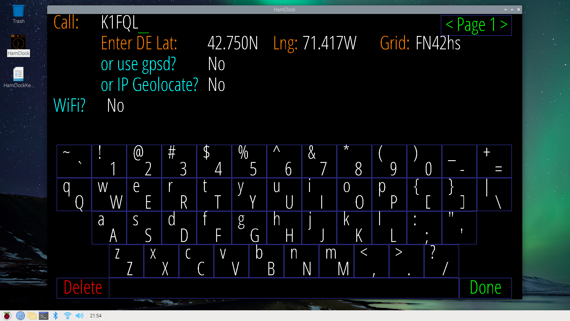 Figure 8. Connect to WiFi Screen. You will enter your call sign on setup page 1. You may provide your network username and password after saying yes to WiFi. If you provided these to the Raspberry Pi operating system, they will auto-fill if you select, yes. You can enter your latitude, longitude and grid square here, or you can Geolocate on your IP address (not recommended). Please click on image to expand.
Once the HamClock screen appears, if the correct resolution has been chosen, the screen should be mostly filled from top to bottom, but there may be some black bars on either side of the window. There are numerous instructions online about how to deal with this. I didn’t bother. Once I had chosen the closest resolution to my screen, 1366 x 768, I left well enough alone. HamClock also asks if you would like full-screen view, Figure 9, which eliminates the HamClock title bar as well as the taskbar. I selected that view.
 Figure 9. Where to Select Full-Screen View. Full-screen view selection is on setup page 5. Please click on image to expand.
To close HamClock, please note that there is a small padlock symbol, Figure 10, beneath UTC in the upper left-hand corner. If one left clicks and holds the lock for a few seconds, then releases, a script will appear that will ask if you would like to exit the program. If you also intend to shut down the Pi, please don’t forget the logout procedure that is found under the Pi logo in the taskbar.
 Figure 10. Padlock Symbol Beneath the UTC Box. If you were to left click and hold on the lock for a few seconds and release, a script will appear that will ask if you would like to exit HamClock. Please click on image to expand.
If you would like HamClock to start automatically upon reboot, a script that will do it may be run anytime from a terminal window. The scripts are found under, ” To install HamClock on other UNIX-like systems follow these steps”, in paragraph 10:
cd ~/ESPHamClock
mkdir -p ~/.config/autostart
cp hamclock.desktop ~/.config/autostart
You may want to place a HamClock icon on your Raspberry Pi desktop. That may be accomplished by copying, pasting and executing the following script in a terminal window:
cd ~/ESPHamClock
mkdir -p ~/.hamclock
cp hamclock.png ~/.hamclock
cp -p hamclock.desktop ~/Desktop
After running the scripts, close the terminal window and reboot the machine from the Pi icon. HamClock should restart immediately. The size of the HamClock window may appear reduced after reboot but may be expanded just as one might expand any other window.
As soon as HamClock is up and running you may want to explore all of the options and items that are found under “Terrain” that is found in the upper left-hand corner of the map, Figure 11. An extensive dropdown menu will appear. Go ahead and press the radio buttons followed by “okay” to see what happens. Every new screen is a surprise. It’s not that hard to get back to the screen where you started, so please experiment a little bit.
 Figure 11. Dropdown Menu for the Main Graphic View. You will want to explore all of the options available from this dropdown menu visible to the left of the Mercator projection. Other menus may be accessed by clicking on the titles that appear within the smaller graphics. For a complete description, please consult the User Guide. Please click on image to expand.
Additional views for the smaller graphics may be requested by clicking on the graphics titles, themselves. For example, you may want to display propagation paths from your locale as supplied by WSJT, Figure 12. There are also satellite and space station orbits.
To change the color of your call sign background, click to the right of your call sign. To change the color of your call sign, click on the letters.
 Figure 12. Display of Propagation Paths From Our Locale. If WSJT-X was selected on Page 2 of the setup menu, this graphic will be displayed. My call sign color and background color has been changed for this view. Please click on image to expand.
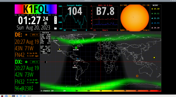
A particularly interesting view of the aurora is shown in Figure 13. This is one more example of how much data is available for presentation in Hamclock.
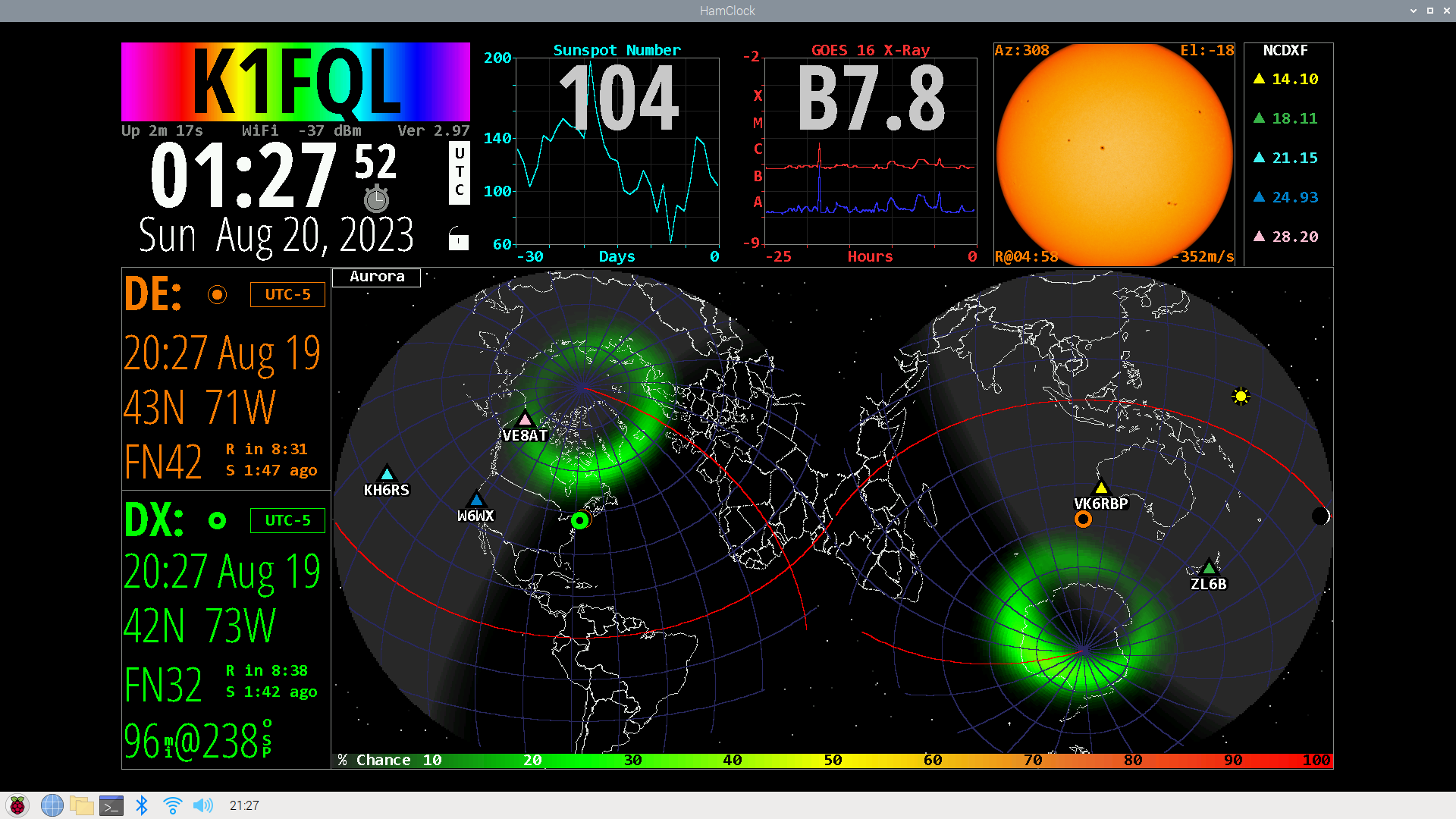 Figure 13. Display of the Aurora. This is another example of how much data is available for display within the HamClock application. Please click on image to expand.
A complete HamClock User Guide is available at the Clear Sky Institute website under the User Guide tab[8].
Please let me know if you build a HamClock of your own. It is nice to receive feedback.
References:
[1] Elwood Downey, WB0OEW, HamClock, QST, October 2017, pp. 42-44.
[2] Raspberry Pi 4, Model B, 2 GB.
[3] Raspberry Pi Zero (2017).
[4] Elwood Downey, WB0OEW, Clear Sky Institute. https://www.clearskyinstitute.com/ham/HamClock/
[5] Jason Oleham, KM4ACK, YouTube, 2:30. https://www.youtube.com/watch?v=2Cy5Swmk3gU
[6] Elwood Downey, WB0OEW, Clear Sky Institute, Op. Cit., Desktop tab.
[7] Jason Oleham, KM4ACK, YouTube, Op. Cit.
[8] Elwood Downey, WB0OEW, Clear Sky Institute, Op. Cit., User Guide tab.