Introduction
Part III of this series is lengthy. It provides the reader with several worked examples in EZNEC that may be helpful. Consequently, the remainder of the topics intended for this installment will be postponed to Part IV. These include methods for hand-calculating radiation resistance, antenna capacitance, antenna ohmic losses from the skin effect, and antenna feed point voltages.
For those of you who would like to use EZNEC, Roy Lewallen, W7EL, has generously made it available, free of charge, to anyone wishing to download it[1].
This section results from a post to the QRZ Technical Forum[2] in which I asked W7EL if he would review the three EZNEC cases that I planned to use to obtain the parameters required to calculate the radiation efficiency for a short, non-resonant vertical antenna.
I received a lengthy response from W7EL and thought-provoking comments from Mike Mladejovsky, WA7ARK[3], and from Dan Maguire, AC6LA, author of AutoEZ[4]. In his response, since it had not been considered, W7EL provided the method for computing the ground reflective loss for the antenna. When the Radiation Efficiency and Reflective Loss are taken together, this shortened, non-resonant vertical is quite inefficient. As will be seen in Part IV, the efficiency is worsened by the resistance of any inductive matching elements that will be necessary at the feed point of this highly reactive antenna.
This article has been largely reorganized to place the results up front and to place the EZNEC models in the Appendices. Appendix A offers a tutorial on how to generate antenna radials. Appendix B, with included comments, provides screenshots of all of the EZNEC cases that contribute to the results.
EZNEC File Recommendations
Based upon their collective recommendations, I altered the three files that I had posted to QRZ Technical Forum: Antennas, Feedlines, Grounding & Towers[5] to eliminate any error messages and departures from the EZNEC User’s Manual by:
1. Moving the source upward to a higher segment of the vertical antenna radiator as shown in the Source Descriptions.
1. Modeling the ground radials at least 0.001 wavelengths above the ground[6] for the NEC-2D engine. (NEC-2D does not provide for buried radials, but NEC-5 does. Since almost no one has a license for NEC-5, all of the calculations in this paper employ the NEC-2D engine.)
2. Following WA7ARK’s recommendation to reduce the radial lengths to match the height of the antenna.
3. Reducing the number of segments in all conductors by using the guidelines provided in the EZNEC User’s Manual[7]. It states that 10 segments are a reasonable number per half wavelength for pattern/gain analysis work. For accurate impedance calculations, 20 segments per half wavelength are reasonable.
4. Ignoring the effects of dielectric insulation losses for radial wires because they are negligible.
These recommendations having been taken into account; seven cases were run. For those of you who are merely interested in the numbers, the cases are summarized in Figure 1, while the feed point impedances are summarized in Figure 2.
Some interesting results are calculated along the way, and some generalized results for antenna efficiency are provided at the end of this article once reflective losses have been addressed.
There is sufficient information provided in Figure 1 to build the models for the seven cases and to reproduce the results tabulated in Figure 2. It is hoped that the reader will follow along to learn more about EZNEC and what it contains. It is also a good exercise for learning how to generate ground radials, and that is covered.
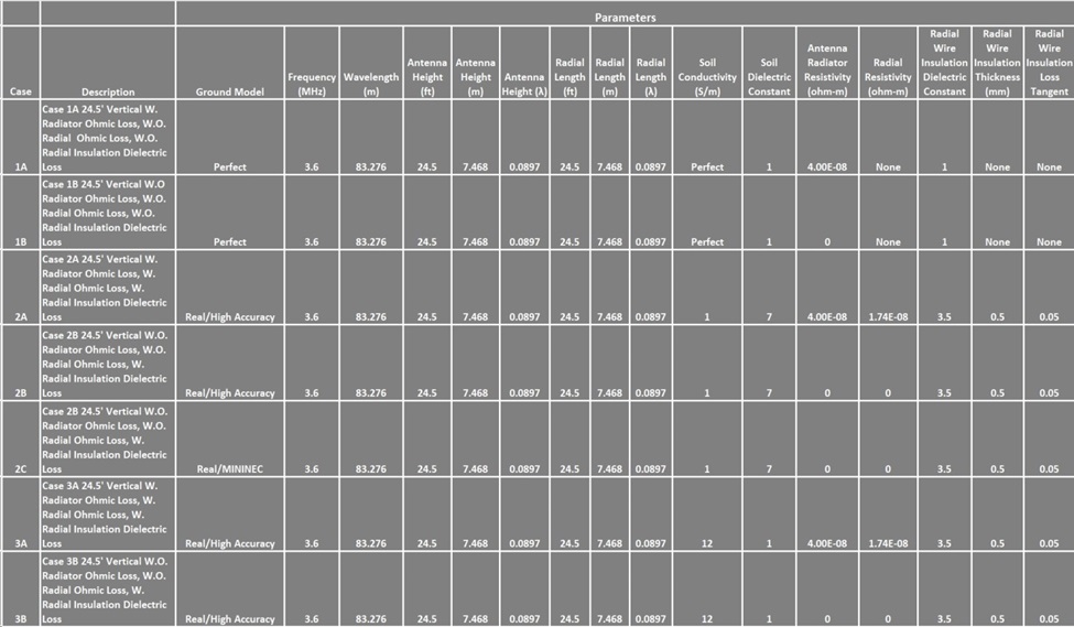 Figure 1. Table of Case Parameters. Seven cases were run to determine the antenna efficiency of a shortened, non-resonant vertical. Please click on the figure to enlarge it.
 Figure 2. Case Summary. Results from seven cases are summarized. This table contains everything required to approximate the antenna efficiency of a shortened, non-resonant vertical antenna. Please click on the figure to enlarge it.
Radiation Efficiency, Ground Reflective Loss, and Antenna Efficiency
Computation of the Radiation Resistance
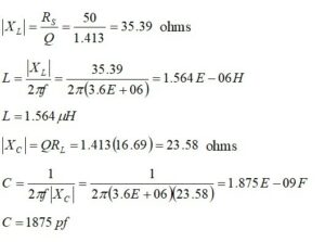
For Case 1B, Plate 4, VSWR Plot, the impedance of the antenna for this case without conductor losses is 3.658 – j519.6 ohms. Compare this impedance with that of Case 1A, Plate 4, with conductor losses, 3.679 – j519.6 ohms. The difference is 21 milliohms which should approximate aluminum radiator RF resistance. Since conductor loss has been removed for Case 1B, and the ground is perfect, the real part of this impedance, 3.658 ohms, should approximate the radiation resistance of this antenna.
Computation of the Ground Loss
For Case 2A, Plate 4, VSWR Plot, the impedance of the antenna for this case is 7.092 – j534.5 ohms. Since Case 1A, real part 3.679 ohms, contains only the resistive losses, and Case 2A, real part 7.092 ohms, contains the resistive and ground losses, the difference should be the ground loss, 3.413 ohms.
Computation of the Ohmic Losses
If we subtract the real part of Case 2B from the real part of Case 2A, the result is 0.026 ohms, the sum of the radiator and radial resistances. If we subtract the real part of Case 3B from the real part of Case 3A, the result is 0.026 ohms. The result is consistent as it should be for the antenna with its radials.
Computation of the Radiation Efficiency
Now that we have the radiation resistance, 3.658 ohms, the ground loss, 3.413 ohms, and the conductor resistance, 0.026 ohms, we can estimate the radiation efficiency of the antenna which does not include any matching inductor loss or any dielectric loss at this time.
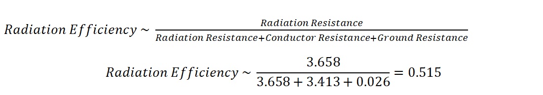
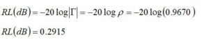
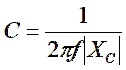
The radiation efficiency for this antenna is approximately 51.5%. Converting to dB, we have,
![]()
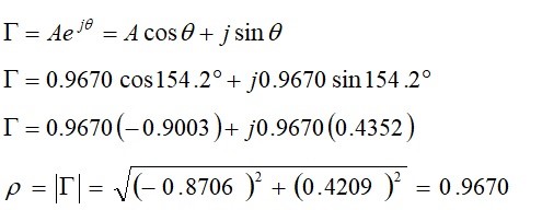
Ground Reflective Loss
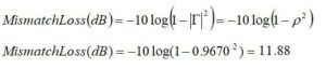
If Case 1C is run with Real/MININEC ground, conductor ohmic loss and ground medium, the average gain is -6.01 dB and this is 5.98 dB down from -0.03 dB for Case 1A with perfect ground and conductor ohmic loss. This is due to the ground reflective loss.
![]()
Antenna Efficiency
Assuming that there is a matching network at the base of the antenna to provide a good match between 50-ohms and this highly reactive antenna, we will, for the moment, ignore ohmic losses in the matching network. We will also ignore polarization losses that increase as the cosine of the angle between the actual and desired polarization.
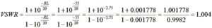
After running Case 2B for Real/High Accuracy Ground, we calculated the radiation efficiency and converted 51.5%, to dB to obtain -2.88 dB. When combined with the ground reflective loss, we obtain:

If we compare this result with that of Case 2A average gain that includes the ohmic and reflective loss minus the Case 1A, perfect ground with ohmic loss, we get -8.83 dB:
![]()
There is agreement between these two results to within 0.03 dB.
Converting the former to percent:
![]()
Converting the latter to percent:

By any measure, this shortened, non-resonant vertical antenna is inefficient.
Final Check
As a final check, if Case 1B with Perfect Ground, zero conductor loss, and with a real part of 3.658 ohms is compared with Case 3B, Real/High Accuracy ground, zero conductor loss, near perfect conductivity at 12 S/m, and with a real part of 3.709 ohms, we conclude that with a difference of only 51 milliohms, there is general agreement. In other words, if Real/High Accuracy ground cases are made to look like near Perfect ground cases by increasing their ground conductivity, the results should be fairly consistent.
References
[1] Lewallen, Roy, W7EL, author of EZNEC Pro+ v. 7.0. https://www.eznec.com/
[2] QRZ Technical Forums, Antennas, Feedlines, Grounding & Towers. K1FQL post: Modeling of Shortened Vertical Antennas in EZNEC, pp. 1 – 3. https://forums.qrz.com/index.php?threads/modeling-of-shortened-verticals-in-eznec.899108/
[3] Mladejovsky, Mike, PhD, WA7ARK, Prof. of EE, Retired, University of Utah.
[4] Maguire, Dan, AC6LA, author of AutoEZ: AutoEZ for EZNEC automation. https://ac6la.com/autoez.html
[5] QRZ Technical Forums, Antennas, Feedlines, Grounding & Towers, op. cit., pp. 1-3.
[6] Lewallen, Roy, EZNEC User’s Manual for EZNEC Pro+ v. 7.0, p. 84. https://www.eznec.com/ez70manual.html
[7] Ibid, p. 64.
Appendix A
Generating Ground Radials in EZNEC – Example
For those who have not generated radials in EZNEC, it is not difficult. We begin with the EZNEC Control Panel as shown in Figure A1. For computations, the frequency has been set to 3.6 MHz. Please note that we begin with a single wire of 10 segments. There is one Source, a Real/High Accuracy has been selected, and the Wire Loss has been set to zero. This means that the radiating element and the ground radial ohmic losses have been set to zero. A ground conductivity of 0.005 S/m and ground dielectric constant of 13 has been selected. Under Plot Type, select 3D. Please try the azimuth and elevation patterns, too.
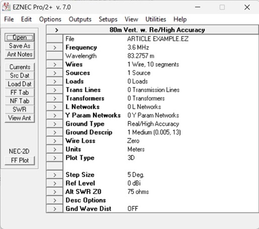
Figure A1. The EZNEC Control Panel. The frequency has been set to 3.6 MHz, the ground type has been set to Real/High Accuracy, and the wire loss has been set to zero. A ground conductivity of 0.005 S/m and a ground dielectric constant of 13 have been selected. Please click on the figure to enlarge it.
The next step is to access the Wires list from the Control Panel by clicking on Wires. A single line is seen in the wire list, Figure A2. The wire radiating element is, in fact, a piece of tubing that is 31.75mm (1.25”) in diameter. The tubing is vertical and runs from End 1 at Z = 0.083m to End 2 at Z=7.551m. If we subtract the two, we see that the vertical radiating element length is 7.468m, the actual antenna length. The lower end of the antenna has been raised to 0.083m (8.3cm) above ground. This is because the radials must be elevated to 0.001 wavelength above ground. The wire segmentation is set to 10 from guidance provided in the EZNEC User’s Manual.
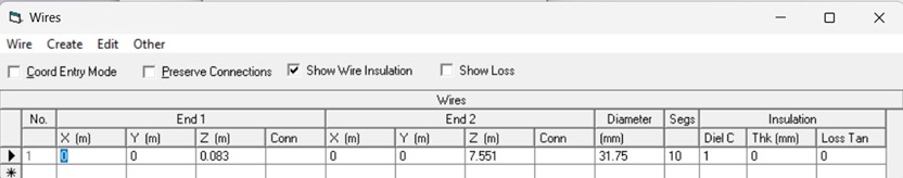
Figure A2. The Wire List. Once selected, the first entry is for the vertical antenna radiator which extends from 0.083m (8.3cm) above ground to 7.551m above ground. The total length of the radiator is 7.468m (24.5 ft). The radiating element consists of an aluminum tube that is 31.75mm (1.25”) in diameter. The conductor resistivity has been set to zero and is not shown. There is no insulation on the tubing, so the dielectric constant is set to 1. The wire segmentation has been set to 10. See text. Please click on the figure to enlarge it.
The next step is to add radials to the Wire List, Figure A3. The radials have to be elevated by 0.083m (0.001 wavelength) to meet the minimum height requirement for the EZNEC NEC-2D engine. Line 2 is the first radial. Since the radials run horizontally, End 1 is at Z=0.083m and End 2 is at Z=0.083m. The radial runs from Y=0 at End 1 to Y=7.468m at End 2. The diameter of #14 AWG wire is 1.638mm. The X-coordinates have been set to zero because they are not used.
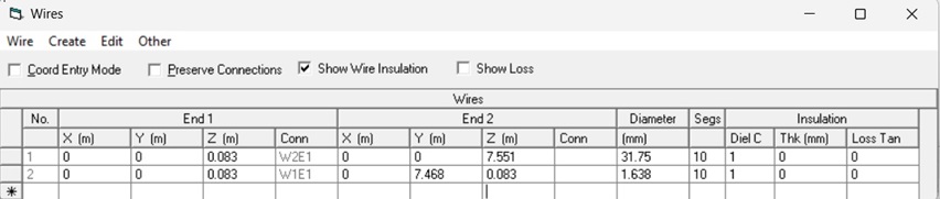
Figure A3. Adding the First Radial Wire. The first radial wire is added to the wire list on line 2. It consists of #14 AWG wire that is 1.638mm (0.0645”) in diameter. It is uninsulated, so its dielectric constant is set to unity. The radials are placed at the minimum required height, 0.001 wavelength, above ground for the ENZNEC NEC-2D engine which does not allow for buried radials. At 3.6 MHz, the wavelength is 83.28m, so the minimum radial height is 8.3cm, or 0.083m. Notice that the radial has been made equal to the height of the antenna, 7.468m (24.5’), and both ends of the radial are 0.083m above ground. The wire segmentation has been set to 10 per the EZNEC User’s Manual. Please click on the figure to enlarge it.
For the sake of example, 10 equally spaced radials will be generated automatically by EZNEC. To do this, a dropdown dialog box is opened under Create, Figure A4. From this list, Radials… is selected.
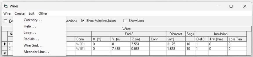
Figure A4. Dropdown Dialog Box. Radials is selected in the dropdown menu. Please click on the figure to enlarge it.
Upon selecting Radials…from the dropdown menu, another dialog box opens, Figure A5. The first line asks us what the first line for the radial prototype is, and the number 2 is entered because it is where the information for the first radial wire has been entered. The second line asks what the last wire in the prototype group is. It is 11 because the first line for the radiator description is counted and 11 is the last radial wire. The third line is just the total number of radial wires, 10. Those lines having been entered; OK is chosen.
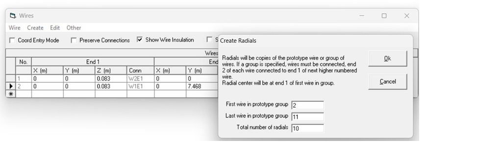
Figure A5. Create Radials Entry. Since the radial wire entries begin with wire 2 in the wire table, the first wire in prototype group is 2. Since there are 10 radial wires, the last wire in the prototype group is 11. The total number of radials is 10. Please click on the figure to enlarge it.
Ten equally spaced radials are generated in the Wires Panel, Figure A6.
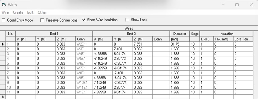
Figure A6. Ten equally spaced radials are listed in the wire table from line 2 to line 11. Notice that the radial on line 5 points in the direction opposite to the one on line 2. Please click on the figure to enlarge it.
Once the wire table is produced, the Source Panel is opened by the user, Figure A7. The source is placed as close to End 1 of Wire 1 as possible. If we remember that for the EZNEC NEC-2D engine, sources are placed in the center of line segments, let’s see what happens if we try to place the source at 0% from Wire 1, End 1. EZNEC automatically places the source at 5% from End 1. Since there are 10 segments, and 20 half-segments, the center of the first segment is 5% as is shown.
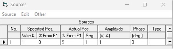
Figure A7. Source Location. The source location is specified in the sources list. As a first guess, we try placing the source 0% from Wire #1, End 1. EZNEC moves it to a point 5% from Wire 1, End 1. This is the center of the first of ten wire segments that make up the vertical. We recall from the EZNEC User’s Manual that sources are placed at the center of wire segments for the NEC-2D engine. Please click on the figure to enlarge it.
Next, in the Control Panel, a VSWR plot is selected. An error message is produced as shown in Figure A8. What’s wrong?

Figure A8. Segmentation Check Error. Everything seems alright, so what’s wrong? Please see text. Please click on the figure to enlarge it.
EZNEC is trying to tell us that the source in the middle of the first segment is still too close to the radial wires. That is because it knows that the first radial and Wire 1, End 1, have been placed 0.083m (8.3cm) above the ground surface. If the source is raised 11% from End 1, EZNEC increases the location of the source to 15%. That is the center of segment 2, Figure A9. EZNEC has to place sources in the middle of segments. We obtain a visual of where it is located when we ask to see what the antenna looks like. If we don’t like the elevated source location, we can try adding more segments to the radiating element so that the source location moves downward even though it will still be centered in Wire 1, Segment 2. Then, if we run a VSWR computation, we can observe if it has a large effect on the impedance, or if there is a diminishing return, as is stated in the EZNEC User’s Manual. Please try changing the number of segments in Wire 1 to see what happens.
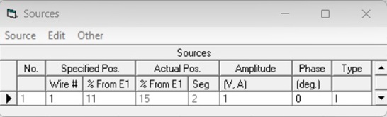
Figure A9. Sources List. As a second try, we move the source 11% from Wire 1, End 1. This places the source in Segment 2. EZNEC reinforces this by moving our choice 15% from Wire 1, End 1, and into Segment 2. We obtain a visual on where it is located when we ask to see what the antenna looks like. Please click on the figure to enlarge it.
We may select a segmentation check from the Options dropdown menu that is accessible from the Control Panel, Figure A10. It confirms that the error message has vanished.
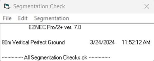
Figure A10. Segmentation Check. Once the source has been moved to a segment that is acceptable to EZNEC, the segmentation check shows ok. Please click on the figure to enlarge it.
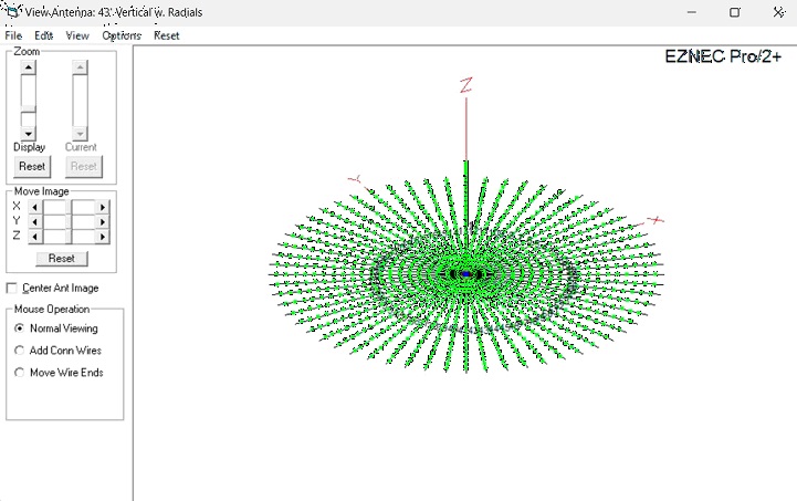
At this point, let’s see what the antenna looks like, Figure A11, by clicking on View Ant on the Control Panel. The source is 1-1/2 segments from the plane of the radials. We’ll see what happens.
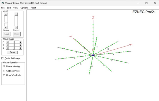
Figure A11. Antenna View. A vertical radiating element is shown with its 10 radials. Both have been elevated to 0.083m (8.3cm) above ground. Please note the position of the source (the tiny red circle) which is plainly visible in the center of the second segment of the vertical radiating element. EZNEC enforces this because we have elevated everything off the ground by 0.001 wavelength. Please click on the figure to enlarge it.
A VSWR Plot may be selected and run from the Control Panel. A dialog box opens, and the frequency range is entered as well as the frequency step interval, Figure A12. Although it is seldom noticed, individual frequencies may be listed in a text file, and these may be called by checking the box that says Read Frequencies From File. This is useful for displaying VSWR data over multiple bands. A named text file must be stored where EZNEC can find it, preferably in the same folder where the EZNEC file has been saved. It is called up by selecting the file name. Please try it. Only discrete frequencies need to be listed. Frequency Step size is not required.
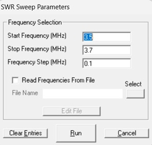
Figure A12. SWR Sweep Parameters. This data entry panel provides start/stop limits for the frequency scan and step granularity. It also provides a means for selecting a frequency data file in which discrete frequency data for a single frequency band, or multiple bands is stored. Please click on the figure to enlarge it.
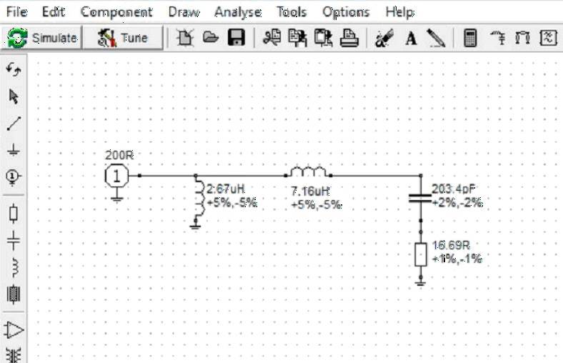
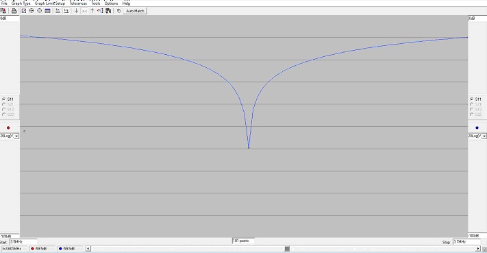
Once we are happy with the Frequency Selection and Frequency Step, Run is selected, and a VSWR Plot appears. Since the antenna has not been matched, and the antenna is highly reactive, the VSWR is astronomically high > 100:1, Figure A13. If we click right on the SWR Plot at 3.6 MHz, the tiny, circular cursor moves to the center of the chart, and the parameters for the calculations appear for the antenna at 3.6 MHz right below the plot. We observe that the impedance of this antenna is computed to be 7.618 – j629.4 ohms. Since this is a short, non-resonant vertical, the real part of the impedance is expected to be low when compared to the ~36.5 ohm real part of a 0.25-wave vertical, resonant monopole above perfect ground. The 629.4 ohm capacitive reactance, indicated by the minus sign on the imaginary part, arises from the fact that the antenna is very short at 3.6 MHz. In Part IV, it will be shown that high feed point reactances give rise to very high voltages, even at low power. The subject of Reflection Coefficient was discussed in detail in a previous post, Blustine, Martin, K1FQL, N1FD post, Worst Case Standing Wave Voltage on a Transmission Line, August 1, 2022. https://www.n1fd.org/2022/08/01/standing-wave-voltage/
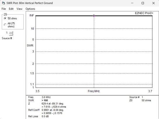
Figure A13. SWR Plot. The SWR is >100:1 for this unmatched non-resonant, vertical antenna. The impedance is 7.618 – j629.4 ohms. The high reactive part gives rise to very high voltages at the antenna feed point. A matching element is required at the feed point to reduce the SWR to a level that can be handled by an automatic antenna tuner, either remote or local. Please click on the figure to enlarge it.
Next, we may request a 2D or 3D antenna pattern from the Control Panel under FF Plot. Let’s request a 3D antenna pattern so that EZNEC will calculate the average antenna gain from the plot, Figure A14.
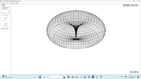
Figure A14. 3D Antenna Pattern. EZNEC plots the 3D antenna pattern for us while computing the average gain for the antenna that will be displayed on the Control Panel once the 3D antenna pattern has been run. Please click on the figure to enlarge it.
If we reduce or close the 3D plot, an average gain computation appears at the bottom of the Control Panel, Figure A15. The average gain for the entire pattern is -6.55 dB. This average is computed from several discrete samples. There is a note that says that the Model contains loss. Even though the conductor ohmic losses are zero, there is still ground loss.
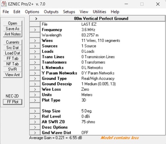
Figure A15. Average Gain Computed from the 3D Pattern. The gain is displayed at the bottom of the Control Panel. Even though conductor losses have been set to zero, the model displays the comment Model contains loss. This is because EZNEC has also computed the ground loss for this antenna. Please click on the figure to enlarge it.
If we were to change the Ground Type in the Control Panel to Perfect, we see that this ground loss disappears because it has not been included in the model, Figure A16. Subtracting -0.01 dB from -6.55 dB, we conclude that the average gain is -6.54 dB for the Real/High Accuracy ground type that includes ground loss. The reason that the average gain for perfect ground does not show as zero is that the calculation is performed by sampling at several discrete points on the pattern.
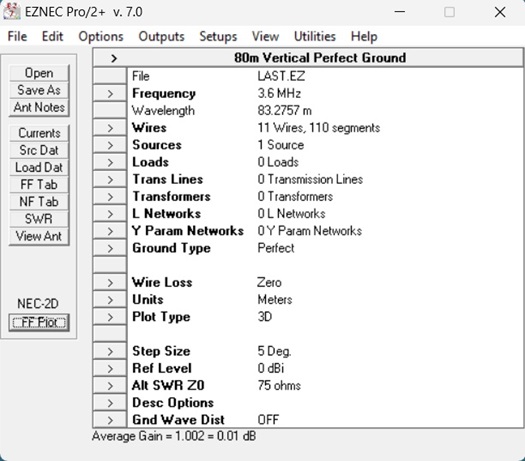
Figure A16. Average Gain Once Ground Type Is Set to Perfect. Reflective loss is not included in this model. The reason that the Average Gain does not say zero is that the average gain is computed for several discrete points on the pattern. Please click on the figure to enlarge it.
Appendix B
Case 1A: 24.5′ Vertical W. Radiator Ohmic Loss, W.O. Radial Ohmic Loss, W.O. Radial Insulation Dielectric Loss
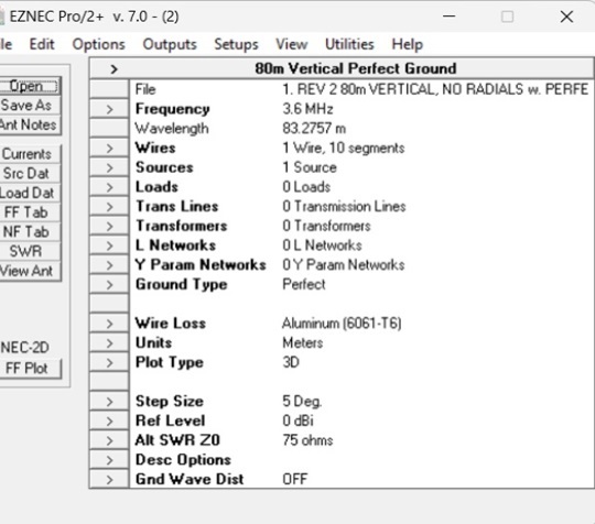 Figure B1. Case 1A, Plate 1, Control Panel for EZNEC. A 24.5′ Vertical with radiator ohmic loss, without radial ohmic loss, and without radial wire insulation dielectric loss has been modeled. The ground type is perfect, and there are no ground radials present. Please click on the figure to enlarge it.
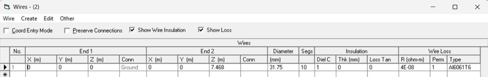 Figure B2. Case 1A, Plate 2, Wire List. Only the aluminum radiator with ohmic loss is present. The ground type is perfect, and there are no ground radials present. Please click on the figure to enlarge it.
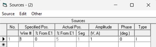 Figure B3. Case 1A, Plate 3, Source Location Description. Note that when there is perfect ground, the source is located near the end of the antenna conductor and close to the ground plane. Please click on the figure to enlarge it.
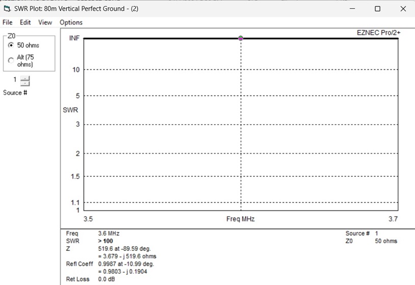
Figure B4. Case 1A, Plate 4, VSWR Plot. The impedance of the antenna for this case is 3.679 – j519.6 ohms. Please click on the figure to enlarge it
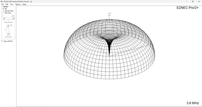 Figure B5. Case 1A, Plate 5, 3D Antenna Pattern. The pattern extends down to the perfect ground conductor. Please click on the figure to enlarge it.
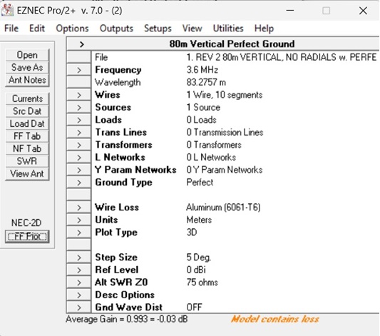 Figure B6. Case 1A, Plate 6. Average Gain Computation. Under Plot Type, 3D is selected. After the 3D pattern has been run, the average gain is computed and reported by EZNEC at the bottom of the Control Panel. Note that for a perfectly conducting ground with conductor loss for the radiating element, the average gain is -0.03 dB. Please click on the figure to enlarge it.
Case 1B: 24.5′ Vertical W.O Radiator Ohmic Loss, W.O. Radial Ohmic Loss, W.O. Radial Insulation Dielectric Loss
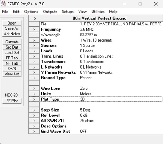 Figure B7. Case 1B, Plate 1, Control Panel for EZNEC. A 24.5′ Vertical without radiator ohmic loss, without radial ohmic loss, and without radial wire insulation dielectric loss has been modeled. The ground type is perfect, and there are no ground radials present. Please click on the figure to enlarge it.
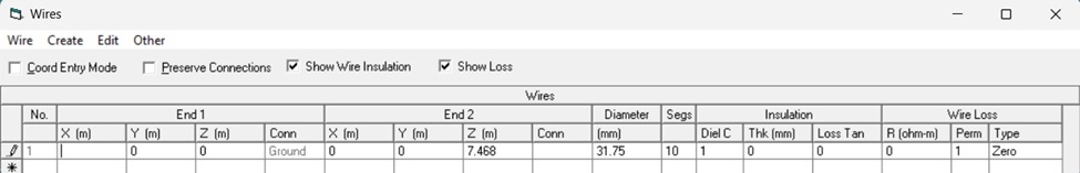
Figure B8. Case 1B, Plate 2, Wire List. Only the aluminum radiator without ohmic loss is present. The ground type is perfect, and there are no ground radials present. Please click on the figure to enlarge it.
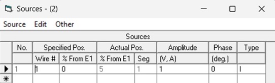 Figure B9. Case 1B, Plate 3, Source Location Description. Note that when there is perfect ground, the source is located near the end of the antenna conductor and close to the ground plane. Please click on the figure to enlarge it.
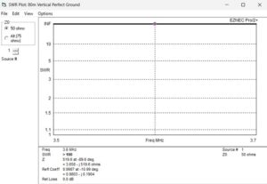
Figure B10. Case 1B, Plate 4, VSWR Plot. The impedance of the antenna for this case without conductor losses is 3.658 – j519.6 ohms. Compare this impedance with that of Case 1A, Plate 4, with conductor losses, 3.679 – j519.6 ohms. The difference is 21 milliohms which should approximate aluminum radiator RF resistance. Since conductor loss has been removed and the ground is perfect, the real part of this impedance, 3.658 ohms, should approximate the radiation resistance of this antenna. Please click on the figure to enlarge it.
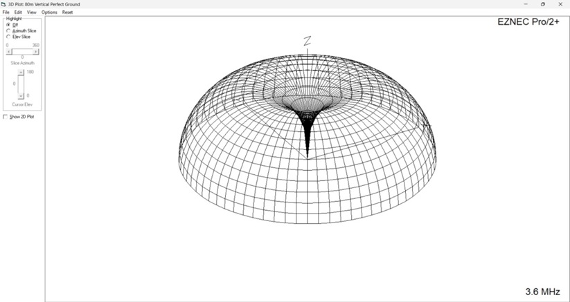
Figure B11. Case 1B, Plate 5, 3D Antenna Pattern. The pattern extends all the way down to the perfect ground conductor. This is characteristic of antennas modeled above perfect, or near-perfect ground conductors. Please click on the figure to enlarge it.

Figure B12. Case 1B, Plate 6, Average Gain Computation. Under Plot Type, 3D is selected. After the 3D pattern has been run, the average gain is computed and reported by EZNEC at the bottom of the Control Panel. Note that for a perfectly conducting ground without conductor loss for the radiating element, the average gain is -0.01 dB. When compared to Figure B6, Case 1A, Plate 6, we may infer that the aluminum radiator loss accounts for an additional 0.02 dB of average gain loss. Please click on the figure to enlarge it.
Case 1C 24.5’ Vertical W. Radiator Ohmic Loss, W.O. Radial Ohmic Loss. W.O. Radial Insulation Dielectric Loss to Compute Reflective Loss
Up to now, only conductor ohmic losses and ground losses have been considered for computing radiation efficiency. There is another type of loss present – reflective loss. This is not to be confused with reflected power which is a different matter. Reflective loss is wasted electromagnetic energy that scatters off the ground and does not propagate in the intended direction.
W7EL, explains in QRZ Technical Forums, Antennas, Feedlines, Grounding & Towers, op. cit., p. 2, that reflections occur far beyond the expanse of any practical radial field that we might have. Consequently, reflective loss has little or no effect on the feed point impedance. The way to separate the reflective loss from other losses is discussed in this section.
Real/MININEC ground uses Real ground for the ground reflective calculation, but not for ground ohmic loss because it uses perfect ground for the current and impedance calculation. Consequently, it provides a means of isolating the ground reflective loss.
Case 1A is repeated with Real/MININEC ground, no radials, radiator ohmic loss, 0.001 S/m ground conductance, and ground dielectric constant 7 to find the average gain. We’ll call it Case 1C. This value is adjusted by the gain for Case 1A having perfect ground and radiator conductor loss. The result is the ground reflective loss.
Thus, if we run Case 1A with Real/MININEC ground, called Case 1C, we obtain the following, Figure B13:
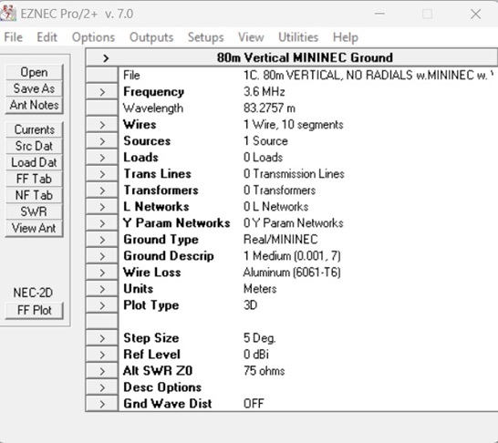 Figure B13. Case 1C, Plate 1, Control Panel. Real/MININEC Ground with radiator ohmic loss and ground medium. Real/MININEC uses real ground for the ground reflective calculation but not the ground ohmic loss because it uses perfect ground for the current and impedance calculation. Please click on the figure to enlarge it.
 Figure B14. Case 1C, Plate 2, Partial Wire List Real/MININEC Ground with Radiator Ohmic Loss. Please click on the figure to enlarge it.
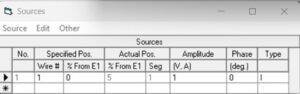
Figure B15. Case 1C, Plate 3, Source Location Description. Note that EZNEC has permitted us to place the source near the end of Wire 1, Segment 1. MININEC does not enforce the placement of the source at the center of wire segments. Please click on the figure to enlarge it.
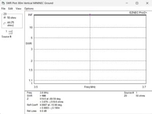
Figure B16. Case 1C, Plate 4, VSWR Plot. Real/MININEC Ground with Radiator Ohmic Loss and Ground Medium. The impedance is 3.679 – j519.6 ohms. Please click on the figure to enlarge it.
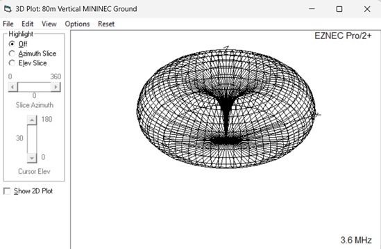
Figure B17. Case 1C, Plate 5, 3D Antenna Pattern. Real/MININEC Ground with conductor loss and ground medium. Please click on the figure to enlarge it.
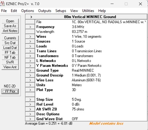 Figure B18. Case 1C, Plate 6, Average Gain for Real/MININEC Ground with Radiator Ohmic Loss and Ground Medium. The average gain is -6.01 dB and this is 5.98 dB down from -0.03 dB for Case 1A that had perfect ground, conductor ohmic loss, and no ground medium. This is due to the ground reflective loss. Please click on the figure to enlarge it.
Case 2A: 24.5′ Vertical W. Radiator Ohmic Loss, W. Radial Ohmic Loss, W. Radial Insulation Dielectric Loss
 Figure B19. Case 2A, Plate 1, Control Panel. A 24.5′ vertical with radiator ohmic loss, with radial ohmic loss, and with radial wire insulation dielectric loss has been modeled. The ground type is Real/High Accuracy, and there are ground radials present. The soil conductivity is poor and the dielectric constant is low. Please click on the figure to enlarge it.
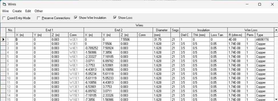
Figure B20. Case 2A, Plate 2, Partial Wire List. A partial wire list for 60 ground radials is shown. Conductivities for the aluminum radiator and copper ground radials are accounted for as is PVC insulation on the ground radials. The radials have been made the same length as the antenna radiating element. Please click on the figure to enlarge it.
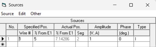 Figure B21. Case 2A, Plate 3, Source Location Description. EZNEC requires the placement of the source in segment 2. Please click on the figure to enlarge it.
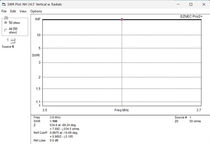
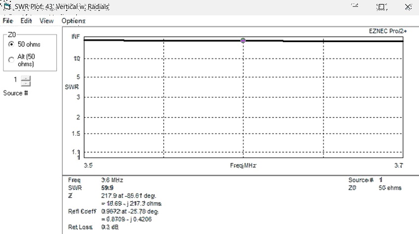
Figure B22. Case 2A, Plate 4, VSWR Plot. The impedance of the antenna for this case is 7.092 – j534.5 ohms. Since Case 1, real part 3.679 ohms, contains only the resistive losses, and Case 2, real part 7.092 ohms, contains the resistive and ground losses, the difference should be the ground loss, 3.413 ohms. Please click on the figure to enlarge it.

Figure B23. Case 2A, Plate 5, 3D Antenna Pattern. The pattern is that of a vertical radiator above imperfect ground. Please click on the figure to enlarge it.
 Figure B24. Case 2A, Plate 6. Average Gain Computation. Under Plot Type, 3D is selected. After the 3D pattern has been run, the average gain is computed and reported by EZNEC at the bottom of the Control Panel. Notice that in the presence of conductor losses, ground losses and dielectric losses, the average gain is -8.86 dB. Please click on the figure to enlarge it.
Case 2B 24.5′ Vertical W.O. Radiator Conductor Loss, W.O. Radial Conductor Loss, W. Radial Insulation Dielectric Loss
 Figure B25. Case 2B, Plate 1, Control Panel. In this model of the 24.5’ vertical with radials above poor conducting soil, we set the conductor loss resistances to zero. Please click on the figure to enlarge it.
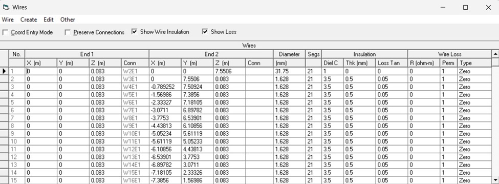
Figure B26. Case 2B, Plate 2, Partial Wire List. A partial wire list for 60 ground radials is shown. Notice that the conductor loss resistances for the radiator and the radials have been set to zero. Please click on the figure to enlarge it.
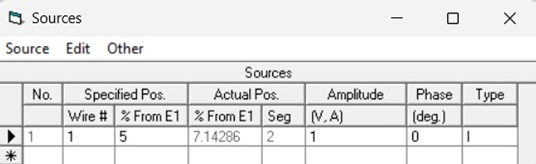 Figure B27. Case 2B, Plate 3, Source Location Description. EZNEC requires the placement of the source in segment 2. Please click on the figure to enlarge it.
 Figure B28. Case 2B, Plate 4, VSWR Plot. The impedance reported is 7.066 – j534.6 ohms where the conductor losses have been set to zero. By subtracting the real part, 7.066 ohms, from the real part of Case 2A, Plate 4, 7.092 – j534.5 ohms, we obtain the loss resistances of the radiator and ground radials, 26 milliohms. Now that we have the radiation resistance, 3.658 ohms, the ground loss, 3.413 ohms, and the conductor loss, 0.026 ohms, we can estimate the radiation efficiency of the antenna which does not include any matching inductor loss or any dielectric loss. Please click on the figure to enlarge it.
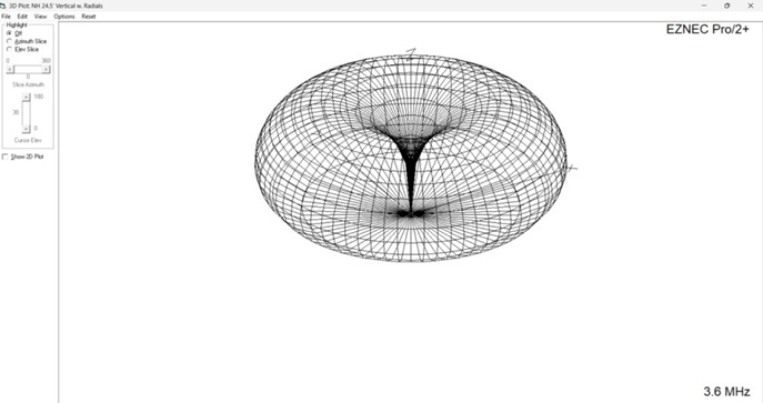 Figure B29. Case 2B, Plate 5, 3D Antenna Pattern. The plot is that of a vertical radiator above imperfect ground. Please click on the figure to enlarge it.
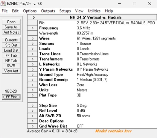 Figure B30. Case 2B, Plate 6, Average Gain Computation. When the conductor loss is removed, the average gain is reported as -8.84 dB. If we compare this result with that of Case 2A, Plate 6, we see that the difference is only 0.02 dB. This result is consistent with that of Case 1. Please click on the figure to enlarge it.
Case 3A 24.5′ Vertical W. Radiator Conductor Loss, W. Radial Conductor Loss, W. Radial Insulation Dielectric Loss
 Figure B31. Case 3A, Plate 1, Control Panel. This time the 24.5’ vertical is operated with radials above highly conductive ground, 12 S/m with a soil dielectric constant of unity. This approximates a near-perfect ground plane even though there are radials present. Please click on the figure to enlarge it.
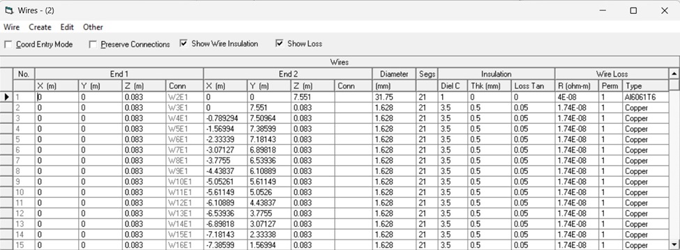
Figure B32. Case 3A, Plate 2, Partial Wire List. A partial wire list for 60 ground radials is shown. Wire losses are included in this calculation. Please click on the figure to enlarge it.
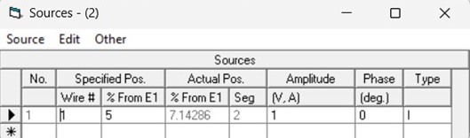 Figure B33. Case 3A, Plate 3, Source Location Description. EZNEC requires the placement of the source in segment 2. Please click on the figure to enlarge it.
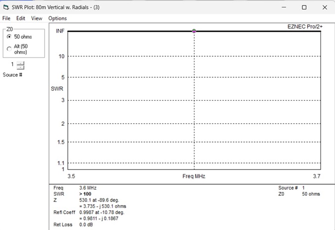
Figure B34. Case 3A, Plate 4, VSWR Plot. The impedance of our 24.5’ vertical with ground radials above nearly perfect ground conductivity is 3.735 – j530.1 ohms. Please note that the real part compares favorably with the result obtained for Case 1A for a 24.5’ vertical with no radials above perfect ground. Please click on the figure to enlarge it.

Figure B35. Case 3A, Plate 5, 3D Antenna Pattern. Note that with ground conductivity set to 12 S/m, the ground conductivity is near perfect. Hence, the pattern appears quite similar to that of the perfect ground plots of Cases 1A and 1B. Please click on the figure to enlarge it.
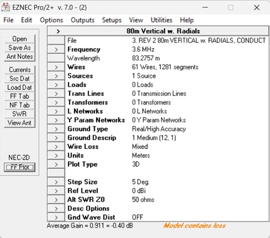 Figure B36. Case 3A, Plate 6, Average Gain Computation. The average gain computation appears at the bottom of the page for near-perfect ground with conductor losses. Please click on the figure to enlarge it.
Case 3B 24.5′ Vertical W.O. Radiator Conductor Loss, W.O. Radial Conductor Loss, W. Radial Insulation Dielectric Loss
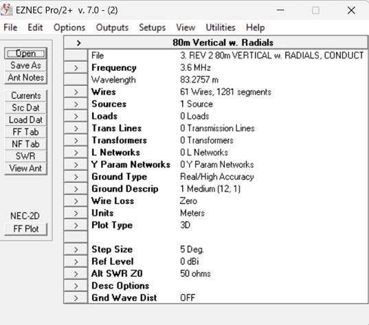 Figure B37. Case 3B, Plate 1, Control Panel. For this exercise, the wire loss is set to zero for the case of nearly perfect ground conductivity. Please click on the figure to enlarge it.
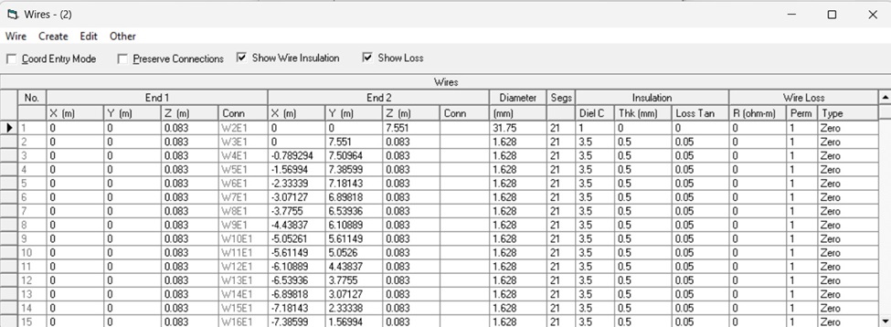 Figure B38. Case 3B, Plate 2, Partial Wire List. A wire list is shown with all conductors set to zero. Please click on the figure to enlarge it.
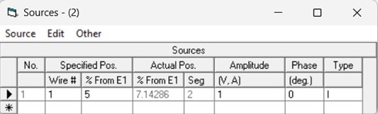 Figure 39. Case 3B, Plate 3, Source Location Description. EZNEC requires the placement of the source in segment 2. Please click on the figure to enlarge it.

Figure B40. Case 3B, Plate 4, VSWR Plot. With the conductor losses set to zero, the impedance is 3.709 – j530.1 ohms. When compared with Case 3A, 3.735 – j530.1 ohms, we see that the difference in the real parts is 0.026 ohms as we have seen before. Please click on the figure to enlarge it.
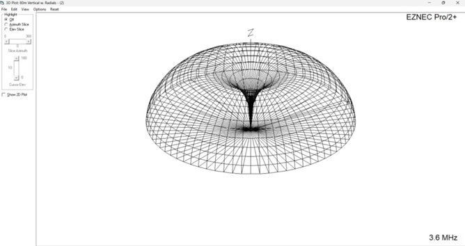
Figure B41. Case 3B, Plate 5, Note that with ground conductivity set to 12 S/m, the ground conductivity is near perfect. Hence, the pattern is quite similar to that of perfect ground. Please click on the figure to enlarge it.
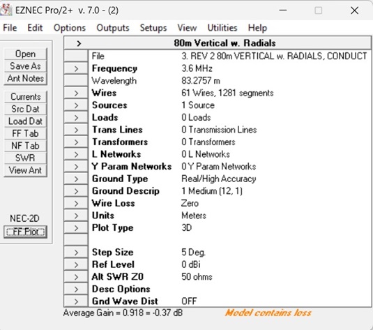 Figure B42, Case 3B, Plate 6, Average Gain. The average gain is reported at the bottom of the page for the case of zero wire loss with the antenna with radials above near-perfect ground conductance. If we compare this gain with that of Case 3A, the difference is 0.03 dB which is consistent with previous results. Please click on the figure to enlarge it.