
In planning for a homebrew QRP SSB transceiver build, it was decided that all of the amplifiers for RF and IF use would be assembled from kits, or purchased preassembled from any of several suppliers in order to save time and money.
The RF to IF Converter described in this article is a good example of how off-the-shelf parts may be packaged to create a working module
The RF to IF Converter is tuned by an SI5351 Clock Generator VFO over the frequency range of 1.1 MHz to 38.7 MHz. This is the VFO frequency tuning range required for high side and low side LO injection to a mixer for 10-band HF operation.
Subassembly List
Mostly off-the-shelf parts that constitute this module are
· a W7ZOI termination insensitive (TIA) amplifier with manual gain control for receive down-conversion [1],
· a W7ZOI termination insensitive (TIA) amplifier with manual gain control for transmit up-conversion [2],
· a Mini-Circuits ADE-1 mixer for receive down-conversion to IF and transmit up-conversion to RF [3],
· W7ZOI bi-directional termination insensitive (TIA) RF amplifier pair with fixed gains for post-mixer receive IF preamplification, and for pre-mixer transmit IF preamplification [4],
· a Bridged-T-Diplexer that provides a 50-ohm termination to the IF port of the ADE-1 mixer [5],
· a Toroidal transformer that transforms the output impedance of the VFO synthesizer from 76-ohms to 50-ohms (see text), and
· a VFO attenuator that reduces the VFO synthesizer drive level to that required by the ADE-1 mixer, +7 dBm [6].
Circuit Descriptions
W7ZOI Termination Insensitive Amplifier (TIA) w. Manual Gain Control
The Wes Hayward, W7ZOI, Termination Insensitive Amplifier (TIA) combines a transistor gain stage, a hybrid cascade (HYCAS) adjustable gain stage, and a two-stage buffer into a single amplifier circuit. Two of these amplifiers are in use on this PCB. They are used as the first amplifier in the receiver and the last amplifier in the transmit chain before the power amplifier. Gain control for this amplifier is designed to work between +1 and +4 VDC, but operation is described down to 0 VDC. At maximum gain, +4 VDC, the gain is 31 dB. In his paper, W7ZOI states that 70 dB of gain control should be possible [7]. For a -30 dBm input signal level at maximum gain, the output should be +1 dBm. W7ZOI notes that there is some gain falloff at higher frequencies. Gain controls for these amplifiers are located on the Control Panel (not pictured).
Mini-Circuits ADE-1 Mixer
A doubly balanced mixer, the Mini-Circuits ADE-1 [8], is used as the RF to IF down-converter upon receive, and the IF to RF up-converter upon transmit. This is a medium LO drive mixer that requires +7 dBm to operate with specs. The nominal conversion loss for this mixer is 5 dB.
W7ZOI Bidirectional Termination Insensitive Amplifier
The W7ZOI Bidirectional Termination Insensitive Amplifier (TIA) differs in architecture from that of the TIA with gain control described above. This amplifier consists of three bipolar transistors in the forward direction and three bipolar transistors in the reverse direction [9]. It has been designed to be termination insensitive in either direction. In this application, the amplifier is biased in the forward direction upon receive and in the reverse direction upon transmit. The nominal gain in each direction is 15 dB. The noise figure of each of the amplifiers was reported to be 5.8 dB by W7ZOI. The output third order intercept point (OIP3) was measured to be +20.5 dBm. The 1 dB compression point was estimated to be +3.5 dBm. This is due to low current transistor biasing. While this intercept point may be adequate for QRP operation, this amplifier won’t win any prizes for dynamic range. This provides an opportunity for future improvement.
Bridged-T Diplexer
In order to obtain the best performance from a doubly balanced mixer, it is vital to terminate all of its ports in 50-ohms. In this application, the RF port “sees” a termination insensitive amplifier. The IF port will also see a termination insensitive amplifier (TIA). I chose to include a Bridged-T Diplexer on the IF port in hopes of improving the mixer performance. The Bridged-T Diplexer consists of 9 MHz series and parallel resonant circuits placed between the mixer IF port and the IF TIA.
Referring to the schematic in Figure 1, the series resonant circuit at the IF frequency of 9 MHz appears to be a low impedance, and it increases to a high impedance away from resonance. The parallel resonant circuit appears like a high impedance at the IF frequency. At frequencies away from the IF frequency, the parallel resonant circuit looks like a low impedance. Consequently, the 50-ohm resistor, R1, to the left, appears across the mixer IF port for frequencies away from the IF frequency. Similarly, for frequencies far from the IF frequency, the TIA amplifier that follows sees the 50-ohm resistor, R2, to the right.

Figure 1. The Bridged-T Diplexer. The series resonant circuit at the IF frequency of 9 MHz appears to be a low impedance, and it increases to a high impedance away from resonance. The parallel resonant circuit appears like a high impedance at the IF frequency. At frequencies away from the IF frequency, the parallel resonant circuit looks like a low impedance. Consequently, the 50-ohm resistor, R1, to the left, appears across the mixer IF port for frequencies away from the IF frequency. Similarly, for frequencies far from the IF frequency, the TIA amplifier that follows sees the 50-ohm resistor, R2, to the right. Please click on the figure to open it in a new window.
In order to design a diplexer of this type, a circuit Q must be specified. Some designs use different Q values for the series and parallel resonant circuits. For this design, Q = 10 was chosen to be the same for both. An online calculator was used to design this Bridged-T Diplexer [10].
VFO Impedance Matching Transformer
It has been determined by direct measurement that the output impedance for an SI5351 synthesizer is not 50-ohms. (The SI5351 Clock Generator output power level and impedance measurement is the subject of a future article.) The measured output impedance does not match the data sheet [11] impedance of 85-ohms at 8 mA bias current. It has been shown that the impedance is closer to 76-ohms at a measurement frequency of 10 MHz, at least for the SI5351 in use. Consequently, the impedance ratio was found to be 1.52:1.
In order to ensure the best possible match, a broadband transformer should be used to perform the impedance transformation if possible. An L-matching network won’t work because the VFO requires a broadband match. Once an FT37-43 toroid core was chosen, the turns-ratio was calculated by taking the square root of the impedance ratio, 1.52:1, resulting in a turns-ratio of 1.233:1. Next, the primary and secondary turns numbers were determined that were as close to whole numbers as possible with the constraint that the winding having the fewest number of turns have an impedance of at least 50-ohms x 5 = 250-ohms.
The turns-ratio that closely matches the requirement is 16T:13T. Dividing the two, obtains 1.231:1. When squared, a value of 1.515:1 is obtained, which is close to the original impedance ratio of 1.52:1.
Next, the impedance of the smaller of the two windings, 13 turns, was checked at the lowest VFO frequency of operation. This is 1.1 MHz for the 30m band. For this verification, a hand calculation can be performed, as has been done in the past, or an online calculator can be used [12]. The result was found to be 409-ohms > 250-ohms, so this winding meets the impedance criterion. Further measurements are required to ascertain that there are no resonances for this transformer over the entire VFO tuning range. Should in-band resonances be encountered, the transformer will be discarded.
A turns-ratio of 11T:9T might also work, but it is not as close a match to the original impedance ratio of 1.52:1. Please check this turns-ratio calculation as an exercise. Also, for practice, please check the 9T winding against the 250-ohm impedance criterion at 1.1 MHz to see if it meets it. Please let me know in the comments section.
VFO Attenuator
The signal output of the SI5351 Clock Generator used to provide the LO to the mixer was calculated and measured to be +11.48 dBm. This would suggest that a ~ 4 dB pad should be used at the mixer LO port input to obtain ~ +7 dBm. If a resistive pad in the PI-configuration is used, the resistor values may be calculated by hand, or an online calculator may be employed [13]. The ~ 4 dB attenuator in Figure 2 uses standard resistor values.
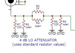
Figure 2. A 4 dB PI-Attenuator. This attenuator uses standard resistor values. They are close enough for this application, where no precision is required. Please click on the figure to open it in a new window.
Schematic Diagram
The schematic diagram of the RF to IF Converter is shown in Figure 3. A pair of manual gain controls (not shown) is provided on the Control Panel. Upon receive, the manual gain control will alter the dynamic range and the receiver noise figure. Upon transmit, the manual gain control will alter the transmitter drive level.
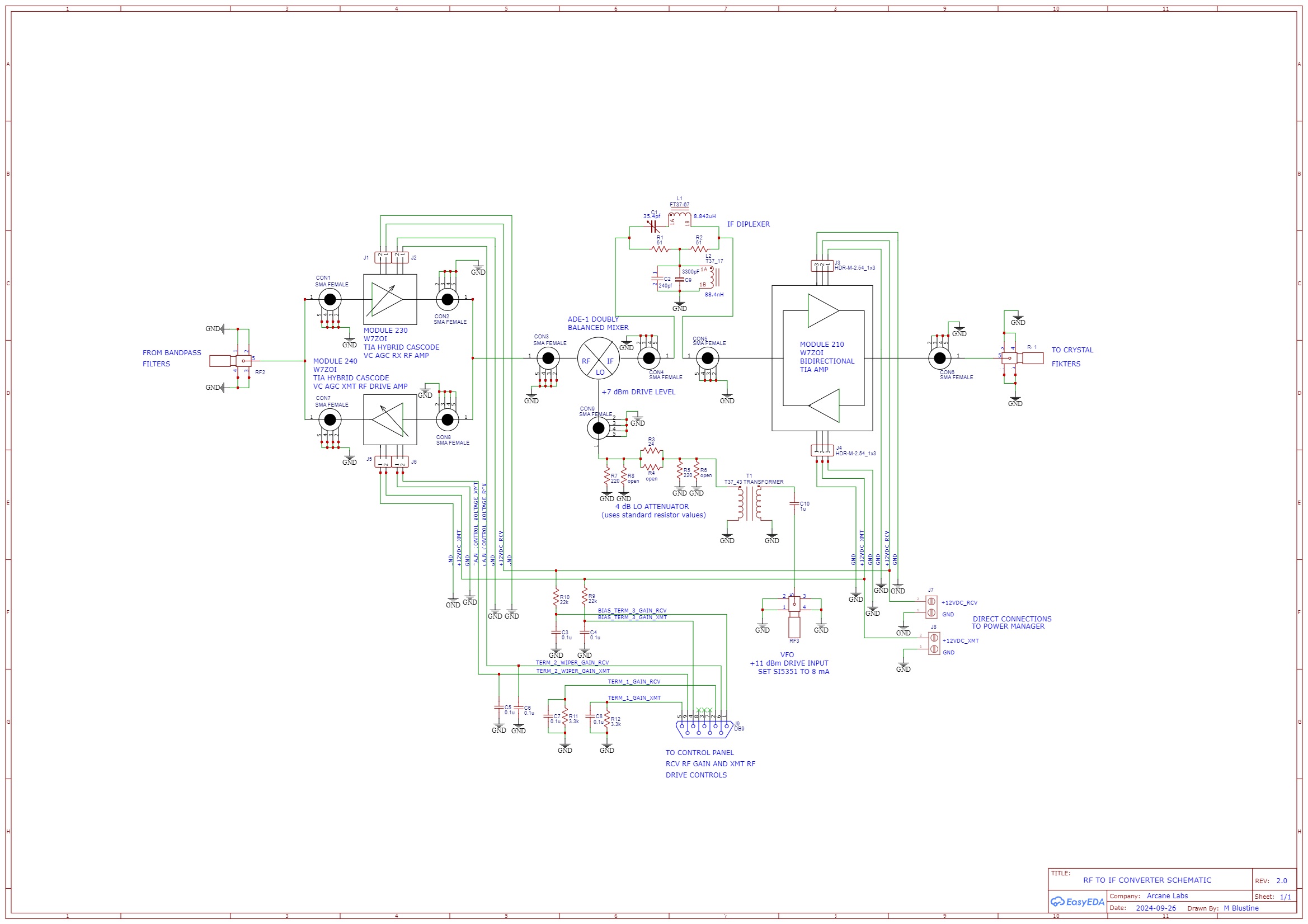 Figure 3. RF to IF Converter Schematic Diagram. This circuit provides RF to IF down-conversion on receive and IF to RF up-conversion on transmit. Manual gain controls are accessible from the Control Panel (not shown). The receive gain control will alter the dynamic range and noise figure upon receive. The transmit gain control will alter the amount of output power upon transmit. Please click on the schematic to open it in a new window.
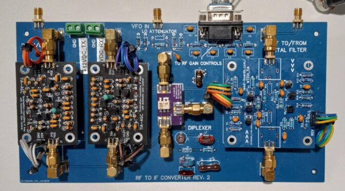
Printed Circuit Board Layout
The printed circuit board layout is shown in Figure 4. Two minor labeling corrections to the PCB are visible since the silkscreen labeling was interchanged. A coupling capacitor, C10, was added to the PCB at the transformer, T1, input. The transformer must be AC-coupled to the SI5351 Clock Generator.
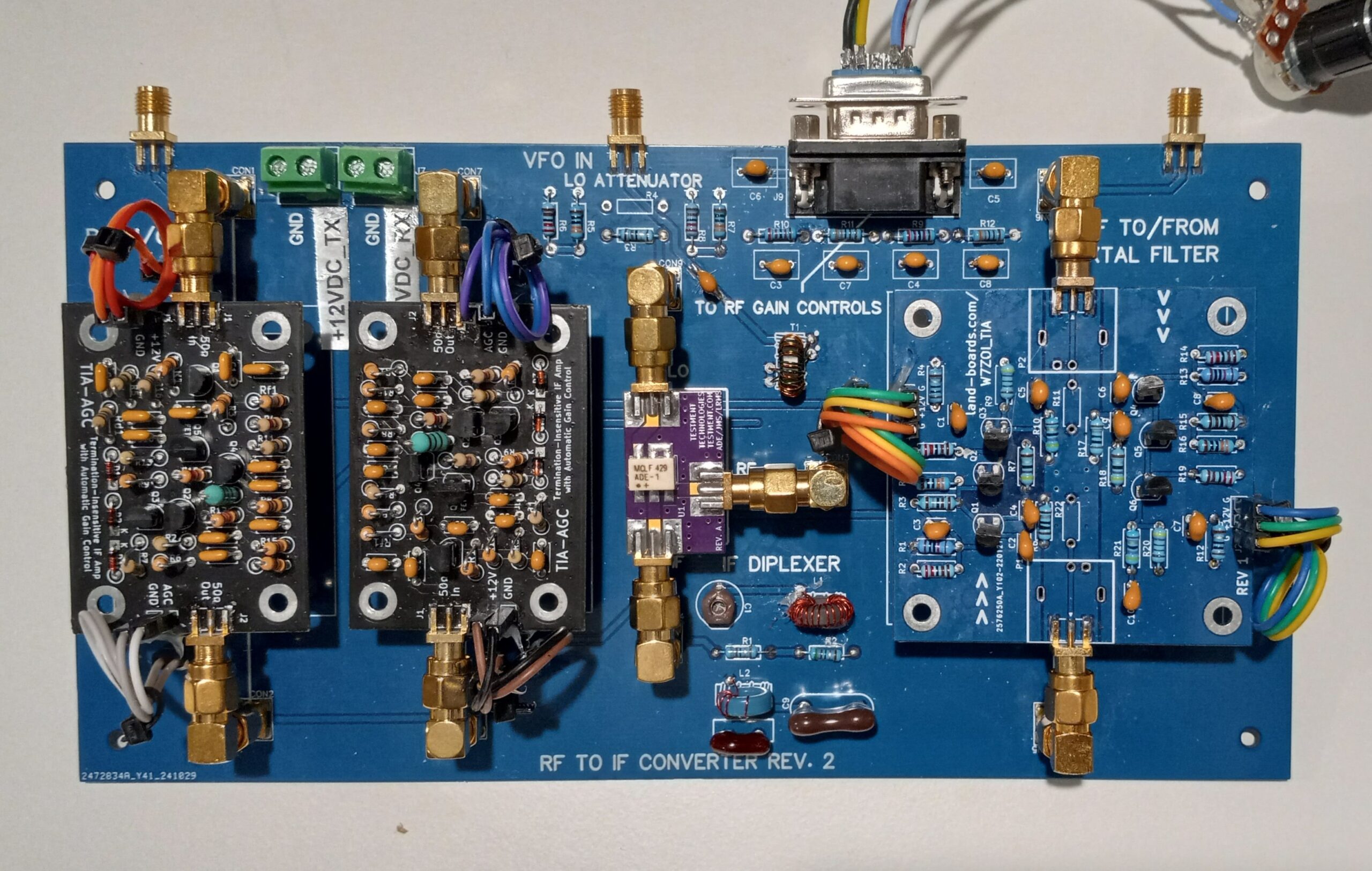
Figure 4. RF to IF Converter PCB. Two W7ZOI Termination Insensitive Amplifiers (TIA’s) with gain control, a Mini-Circuits ADE-1 Doubly Balanced Mixer, and a W7ZOI Bidirectional Termination Insensitive Amplifier (TIA) provide RF gain control and conversion to a 9 MHz IF on receive and from 9 MHz IF to RF on transmit. A Bridged-T Diplexer tuned to 9 MHz provides a constant 50-ohm termination at the IF port of the mixer. Please click on the photo to open it in a new window.
References
[1] Carney, Todd, K7TFC, Mostly DIY RF. https://mostlydiyrf.com/tia-agc/, and https://mostlydiyrf.com/wp-content/uploads/2023/12/TIA-AGC_manual.pdf, and https://w7zoi.net/tia+agc.pdf
[2] Ibid.
[3] CalOutlet. https://www.ebay.com/itm/135758562145?itmmeta=01K1GR7N4T7T8MPD3QGCY00E4T&hash=item1f9bd74361:g:IzMAAOSwxVVoFn7M
[4] Land-Boards, LLC. https://www.tindie.com/products/land_boards/termination-insensitive-rf-amplifier/, and https://w7zoi.net/bidirectional_matched_amplifier.pdf
[5] Bridged-T Diplexer Calculator. https://www.changpuak.ch/electronics/calc_16a.php
[6] PI-Attenuator Design Calculator. https://leleivre.com/rf_pipad.html
[7] Hayward, Wes, W7ZOI. https://w7zoi.net/tia+agc.pdf
[8] Mini-Circuits ADE-1 mixer. https://www.minicircuits.com/pdfs/ADE-1.pdf?srsltid=AfmBOorxmabfezmF18FfPBt4-gGTfS8pEvwuLJuSS6lKZoLp0jG9YTk1
[9] Wes Hayward, W7ZOI. https://w7zoi.net/bidirectional_matched_amplifier.pdf
[10] Bridged-T Diplexer Calculator, Op. cit. https://www.changpuak.ch/electronics/calc_16a.php
[11] Silicon Labs Data Sheet, p. 4. https://cdn-shop.adafruit.com/datasheets/Si5351.pdf
[12] Toroidal Inductor Calculator. https://toroids.info/FT37-43.php
[13] PI-Attenuator Design Calculator, Op. cit. https://leleivre.com/rf_pipad.html
Disclaimers:
The circuits included on this PCB were sourced from a number of authors. Only the 4-channel MUX decoder is original work. This is a somewhat advanced and expensive project, and some prior design and construction experience is recommended before taking on a project of this magnitude. This circuit design is provided for informational and educational purposes only and is supplied “as is” and without warranties of any kind, express, implied, or statutory. No representations or warranties are made regarding the accuracy, adequacy, completeness, legality, reliability, or usefulness of this information, either in isolation or in the aggregate. This circuit design may contain links to or information based on external sources or third-party content. Endorsement and responsibility for the accuracy or reliability of such third-party information or for the content of any linked websites are not taken.
_ZX-SSB-II_Audio_Mic_Amp.png)
_ZX-SSB-II_S-Meter.png)