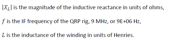
Introduction
An amateur radio transceiver will often require at least two crystal bandpass filters; one for SSB, and another for CW operation. This article discusses impedance matching techniques for a SSB crystal filter to be used in a homebrew QRP transceiver. For a CW filter, the bandwidth would be narrower, but the design process for a matching network would be the same.
Crystal Filter Project Description
When this project began in 2017, there was nothing but a bag of fifty 9 MHz crystals ordered from DigiKey[1]. In retrospect, it might have been more cost-effective to buy a few more of these crystals to get the job done for SSB and CW filters.
Not wanting to bother measuring the crystal motional parameters to enter into DISHAL[2][3]; a simpler approach was adopted[4] which was to sort the crystals into batches of crystals differing in frequency by not more than 10 percent of the desired filter bandwidth. For an SSB filter having a bandwidth of 2.7 kHz, the prescription is to find crystals that are all within 270 Hz of one another. For a 500 Hz wide CW filter, the task becomes more difficult because it requires crystal matching to better than 50 Hz.
Subsequently, I built a crystal oscillator circuit for the purpose of sorting crystals into batches. I chose to follow the advice of Charlie Morris, ZL2CTM, who had done the same [5]. I used the receiver in my rig to measure the frequencies of oscillation by zero beating the crystal oscillator against a signal generator since I didn’t own a frequency counter until recently. I also zero-beat the crystal oscillator against an SDR receiver BFO to compare the crystals to one another. There was lots of advice to be found online about “this and that” including how to handle the crystals with tweezers to avoid heating them up[6].
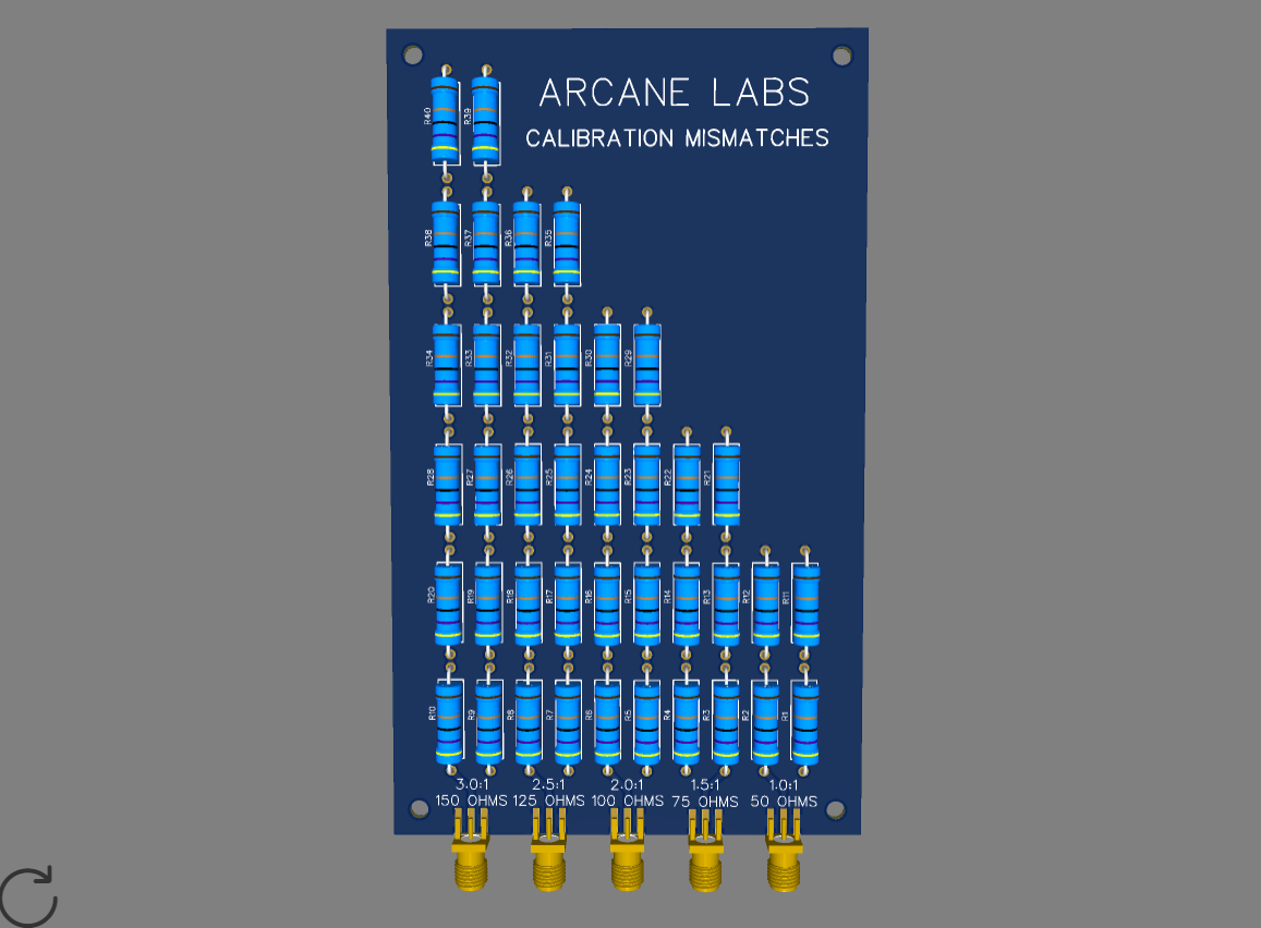
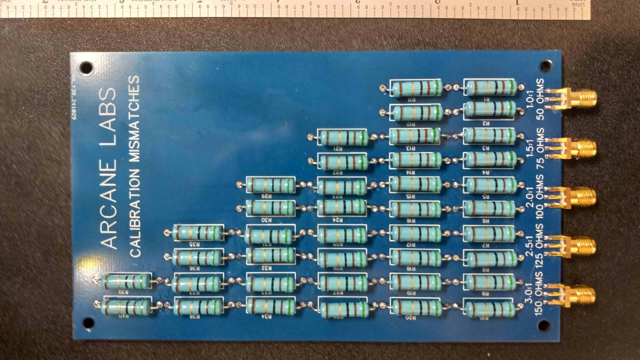
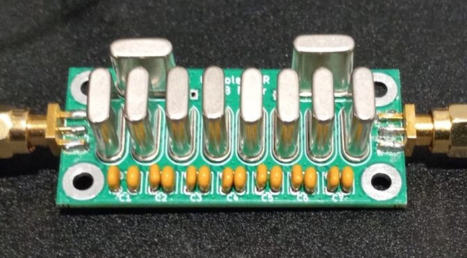
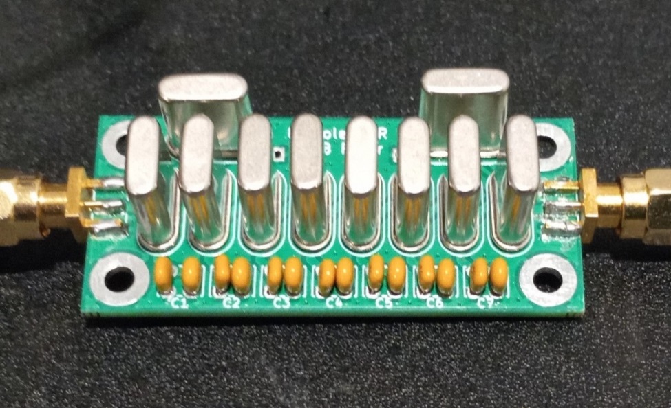
For the batch of 50 Citizen crystals[7] that I sorted, I was not successful in obtaining a set of 10 crystals that met the frequency matching criteria. Thinking that I didn’t want to invest in more crystals, I decided to look for a filter kit whose crystals had already been sorted[8] and whose capacitors had been chosen. There are at least two sources of supply for crystal filter printed circuit boards; one requires the purchase of a set of matched crystals[9] and features places for onboard matching, and another requires an external matching network[10]. I bought a bare board from the former to build a CW filter and a fully populated board from the latter for the SSB filter. A picture of the beautifully made filter from the latter is shown in Figure 1. The filter was characterized by the supplier and came with the following test data:
- Center Frequency: 8.997500 MHz
- 3 dB Bandwidth: 2.7 kHz
- In/Out Impedance: ~160 ohms
- Insertion Loss: 2.65 dB
- Bandpass Ripple: < 1.2 dB
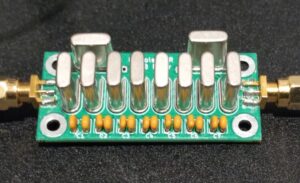
Figure 1. An 8-Pole Quasi-Equiripple (QER) Bandpass Filter. SMA male connectors were added to the device as supplied. No matching networks were furnished for the filter input or output. The supplier advises that matching may be achieved through the use of matching transformers or L-matching networks. Please click on the figure to enlarge it.
Crystal Filter Matching With Matching Transformers
Assuming that the supplier has already determined the best match by placing potentiometers in series with the input and output of the filter to optimize the filter shape, I relied upon their measurement of ~160 ohms as a starting point.
This is a commonly used technique. The potentiometers are adjusted for the best filter passband and stopband shape by sweeping the filter with a nanoVNA, or by viewing the passband response on a spectrum analyzer using an integral tracking generator. Once the potentiometers have been adjusted for the best passband and stopband shape, the potentiometers are measured and 50 ohms is added to each value. This is because the source impedance during the measurement is assumed to be 50 ohms as is the load impedance.
Since I wanted to match the crystals to a 50 ohm system for my QRP rig, I knew that the impedance ratio of the matching network had to be 50:160, or 1:3.2, at the input and 160:50, or 3.2:1, at the output. Since I was going to try a matching transformer for the first pass, I knew that this impedance ratio was not the same as the required turns ratio. To obtain the turns ratio, we must take the square root of the impedance ratio, 3.2, to obtain 1.79. Thus, the turns ratio is 1-turn to 1.79-turns at the input and 1.79-turns to 1-turn at the output.
It is not possible to build a transformer with this turns ratio since only a whole number of turns is possible. Also, we must have a sufficient number of turns on the primary to avoid loading the source. A rule-of-thumb is to ensure that the impedance of the smallest winding is > 5 times the lowest impedance that must be matched. That dictates that the smallest winding must have an impedance of 50 ohms x 5 = 250 ohms at 9 MHz. Next, we use an iterative approach to find the smallest number of turns that will meet our requirements. We do this because the more turns we add, the more the inter-turn capacitance increases. This adds to the complexity of the matching solution. We must always use integer numbers of turns for both windings, so we will seldom get the exact ratio required.
Example 1 – 1-Turn to 2-Turns
If we were to round the 1:1.79 turns ratio to a whole number ratio, we ask, how close would a 1-turn to 2-turn transformer come to meet our requirements? First, we look at the impedance ratio for 1T:2T. It is simply the square of the 2-turn winding, or 4. So, this 1T:2T winding will match 50 ohms to 200 ohms which isn’t a very good match at all. Please, recall that we needed to match 50 ohms to 160 ohms. We also look at the impedance of the smallest winding to see if the magnitude of the impedance is > 5 x 50 ohms, or 250 ohms.
Assuming that the winding is purely inductive, it has an impedance magnitude given by
 where,
 Since the transformer ferrite material is FT37-43, how is the inductance for a 1-turn winding determined?
The manufacturer of the ferrite frequency supplies a factor for a specific core that, when multiplied by the square of the number of turns, will approximate the inductance of the winding. This factor is called AL.
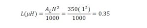
If we study the manufacturer’s data[11] for a FT37-43 core having part number 5943000201, we learn that the AL factor is 350 nH/N2 +/-20% for #43 ferrite of FT37 dimensions.
When we have AL, the formula for inductance for a single turn in units of µH, after converting from units of nH to µH, is given by,
where,
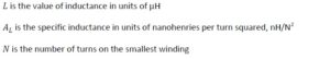
Finally, the value of the magnitude of impedance is calculated from,
This value is not large enough to meet our reactance requirement of > 250 ohms.
Once you have mastered this process, you may wish to employ an online calculator[12].
We could repeat this exercise for other turn ratios by repeating the process, but to save some time, let’s try a ratio of 5-turns to 9-turns in the next example. The reader should try some other turns ratios to better understand the process. For example, try a ratio of 3-turns to 5-turns to see what happens.
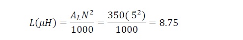
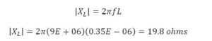
Example – 5-Turns to 9-Turns
A ratio of 5-turns to 9 turns results in an impedance ratio of,

which is close the value, 3.2, that was calculated initially, and

Let’s try this turns ratio of 5T:9T because it results in a value that is close to the desired 160 ohms.
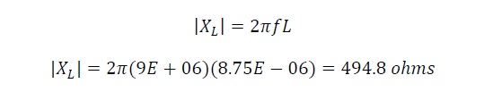
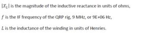
Next, we repeat the process by calculating the reactance of the 5-turn winding since it is the smaller of the two windings. We must first calculate the inductance,
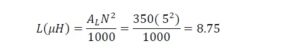
From this value of 8.75 µH, we now calculate the magnitude of the inductive reactance at 9 MHz from,
This result is greater than our 250-ohm requirement, and it will work for us.
Matching Transformer Simulation
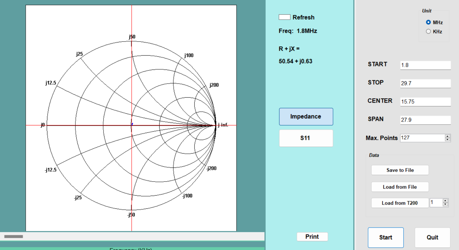
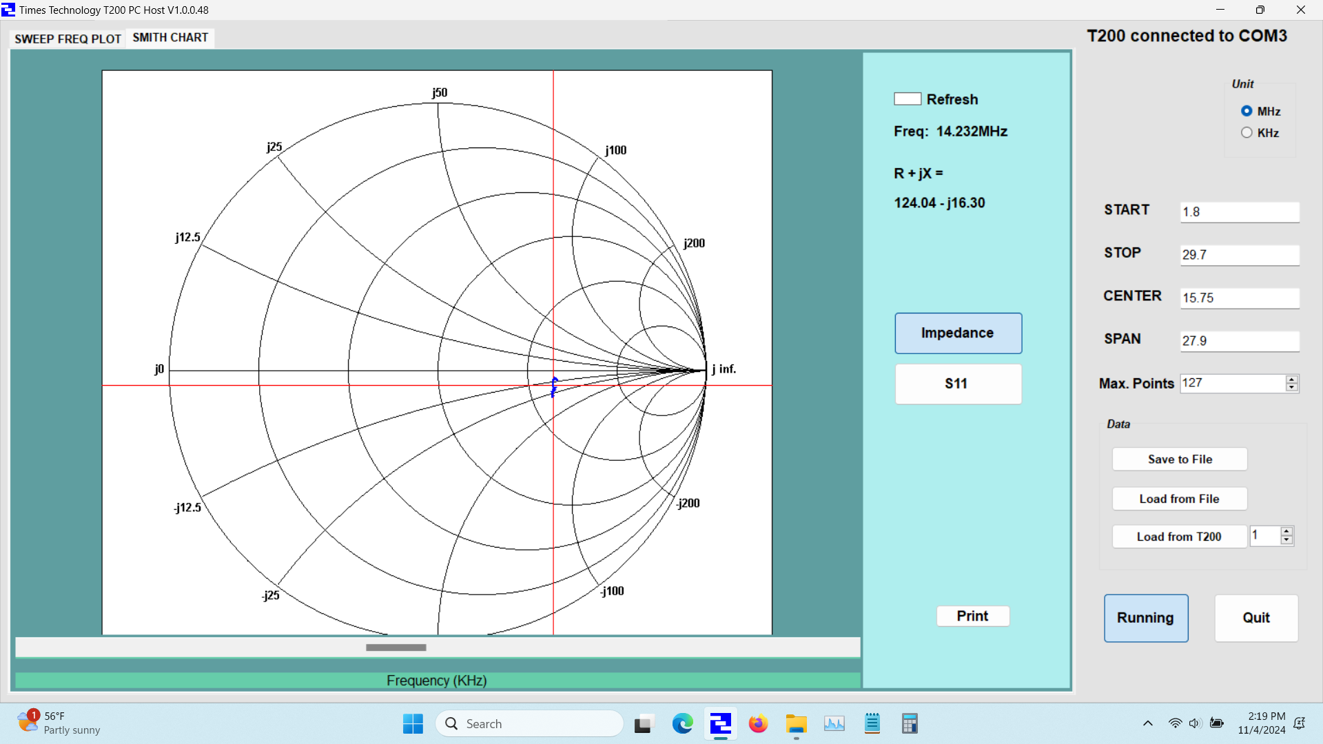
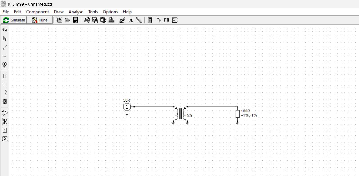
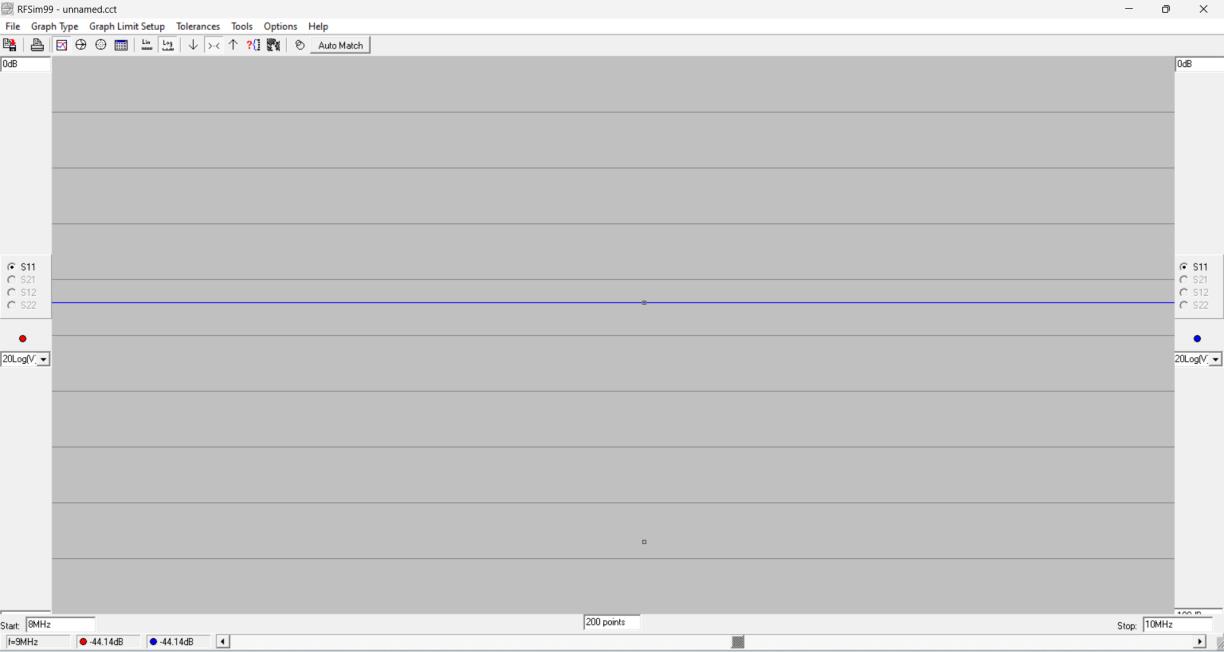
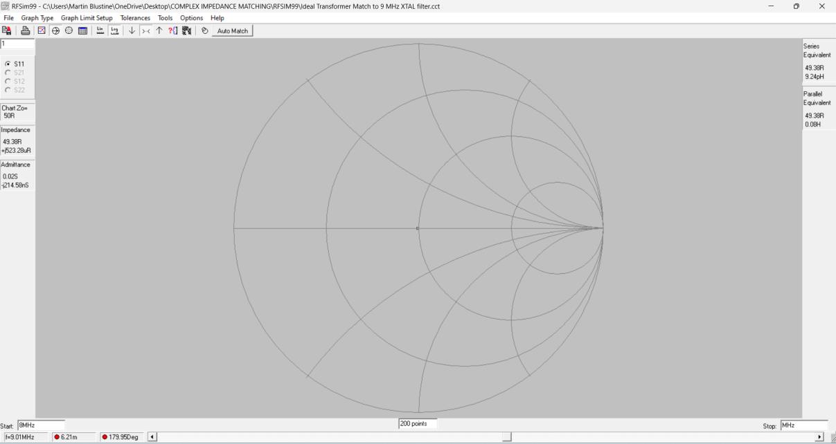
The matching transformer may be simulated using RFSim99[13]. The transformer model is shown in Figure 2. It is modeled as an ideal transformer for which there is no frequency component or coupling factor, k. A rectangular plot of the return loss of the transformer is shown in Figure 3. Since there is no frequency component, the return loss of 44.14 dB is flat for all frequencies. The turns ratio of 5T:9T results in a match between 50 ohms and 162 ohms, a slightly imperfect match for the 160-ohm load. A Smith Chart plot of the match is shown in Figure 4. If the photo is magnified, the cursor appears very close to the center of the chart for all frequencies.
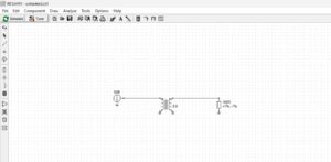
Figure 2. Matching Element Consisting of an Ideal Transformer. A turns ratio of 5T:9T is an imperfect match to 160 ohms. A perfect match would be to 162 ohms. Please click on the figure to enlarge it.
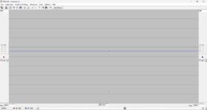
Figure 3. Return Loss for the Ideal Transformer Matching. Since there is no frequency component to an ideal transformer, the match is flat over all frequencies. The return loss is 44.14 dB due to the slight turn ratio mismatch. Please click on the figure to enlarge it.
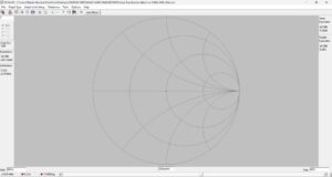
Figure 4. Smith Chart View. Since the simulation is for an ideal transformer possessing no frequency dependence, the cursor resides near the very center of the chart over a wide span of frequencies. Please click on the figure to enlarge it.
Matching Transformer Hardware
Thinking that the matching transformers might be permanently connected to the crystal filter; a printed circuit board was designed using EasyEDA, an online PCB design tool. The Gerber file for the design was transferred electronically to a fabricator, JLCPCB, in Hong Kong, and finished boards were delivered by DHL within 5 days.
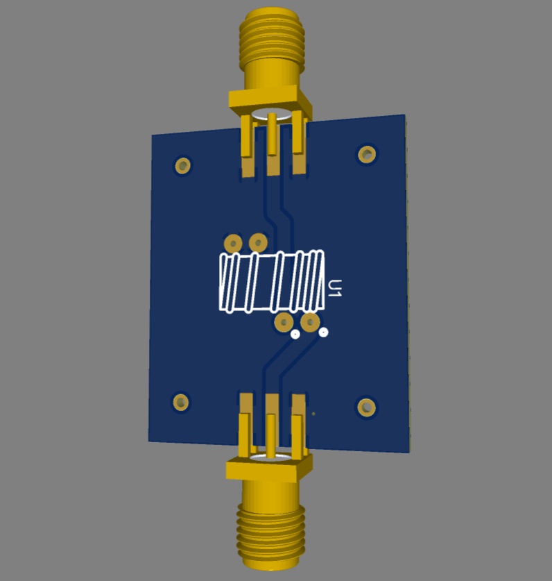
The 3D virtual design is shown in Figure 5. Two Fair Rite FT37-43 toroidal cores were wound with #27 AWG magnet wire, each with a 5-turn primary and a 9-turn secondary. They were wound in no particular sense in mind except to match symbol pattern imprinted on the silk screen. Spoiler Alert: If you are like me, there is a 50-50 chance of winding it the right way the first time around.

Figure 5. Matching Transformer PCB Design. Notice that the center pins of both SMA connectors are routed to the dotted pads. The center conductor from the top SMA connector is routed under the toroid. The undotted pads above the toroid are ground pads for both windings. Thus, the windings, though unequal in number, happen to be wound in the same sense. The EasyEDA design tool provides these 3D virtual views of the finished product. There is a massive library of symbols contributed by users, so there is seldom a need to draw any of them. The only caveat is for multi-pin connectors. There are instances where the schematic model pinouts do not match the PCB graphics model pinouts, and EasyEDA advises the designer to verify the models before using them. Please click on the figure to enlarge it.
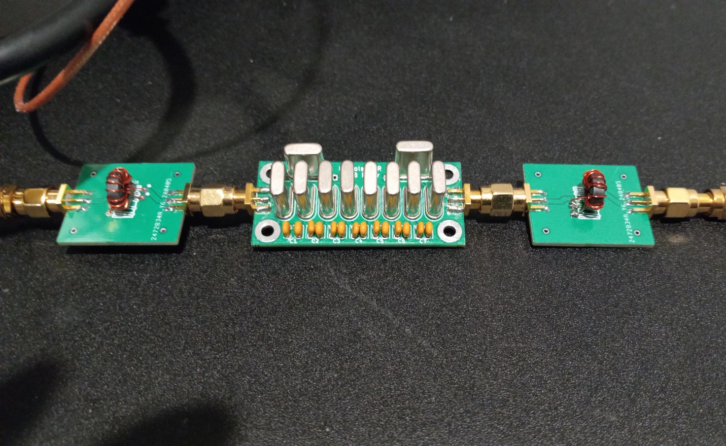
The resulting transformers are shown in Figure 6. No difficulties were encountered with assembly and the PCBs and transformers worked exactly as intended.
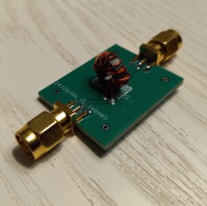
Figure 6. Matching Transformer Assembly. The two windings just happen to be wound in the same sense to match the silkscreen outline on the printed circuit board. The smaller winding has been wound right over the larger winding. Once assembled it is easy to lose track of which end of the transformer is 50 ohms and which end is 160 ohms. One should always mark the 50-ohm end with indelible ink. Male SMA connectors are used to avoid unnecessary cables and adapters between modules. Please click on the figure to enlarge it.
Crystal Filter Measurements
The passband and stopbands of the matched filter were measured with a spectrum analyzer with an integral tracking generator. A tracking generator is a signal source whose RF output follows the tuning of the spectrum analyzer. It could just as well have been measured with a nanoVNA that does the same thing, but I do not own one. The values of center frequency, bandwidth and insertion loss agree quite closely with the values provided by the supplier. The tracking generator outputs -10 dBm, so everything is measured relative to this power level. The coaxial cables that connect the tracking generator to the filter and the filter to the spectrum analyzer are 18” in length. No padding attenuators have been inserted in either the input path or the output path of the device under test (DUT). The test setup is shown in Figure 7. The through-path loss is zeroed out before inserting the device under test which in this case includes the crystal filter with its two matching transformers.
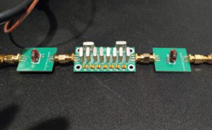
Figure 7. Test Setup For Filter Passband and Stopband Measurements. Nearly identical matching transformers have been placed at the input and output ports of the filter. The transformer to the left steps up the impedance from 50 ohms to 162 ohms, while the transformer to the right steps down the impedance from 162 ohms to 50 ohms. Neither of the 18” interconnecting coaxial cables has been padded. The through-path losses have been zeroed out before inserting the device under test. Please click on the figure to enlarge it.
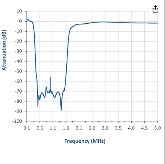
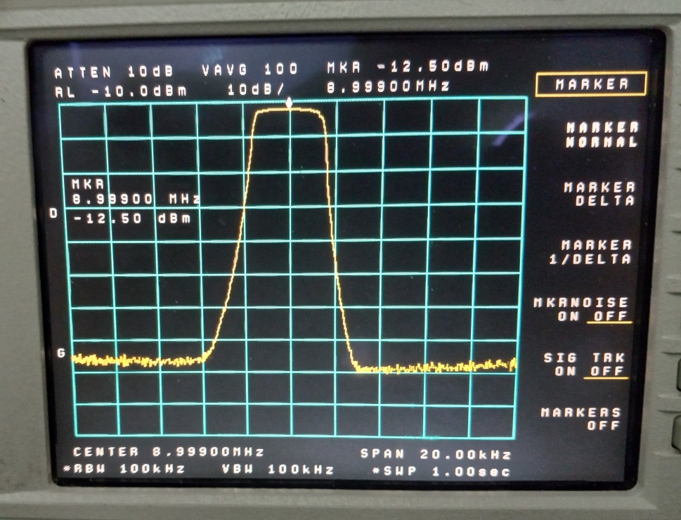
The filter passband was swept with the tracking generator to evaluate the insertion loss of the filter. The losses of cables and adapters have been zeroed out. The insertion loss shown in Figure 8 agrees closely with that measured by the supplier ~ 2.65 dB. The filter center frequency differs slightly from that reported by the supplier, but that is accounted for by the state of instrument calibration and instrument settings.

Figure 8. Crystal Filter Swept Measurement. The filter passband was swept with the tracking generator to evaluate the insertion loss of the filter. The losses of cables and adapters have been zeroed out. The insertion loss agrees with that measured by the supplier at band center ~ 2.65 dB. Please click on the figure to enlarge it.
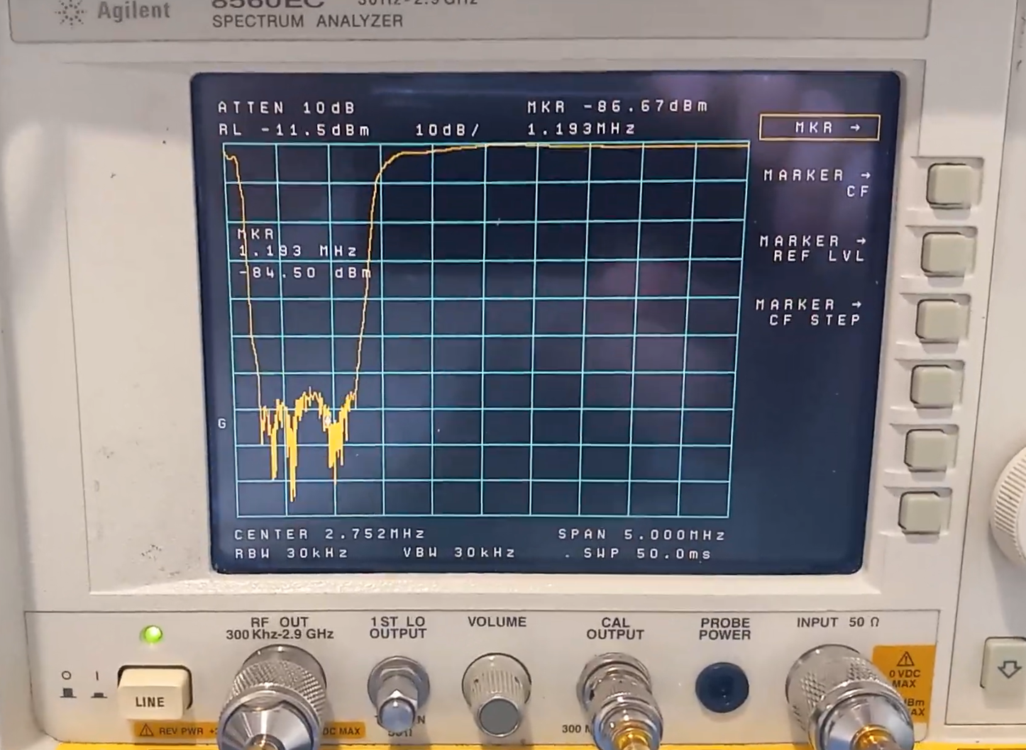
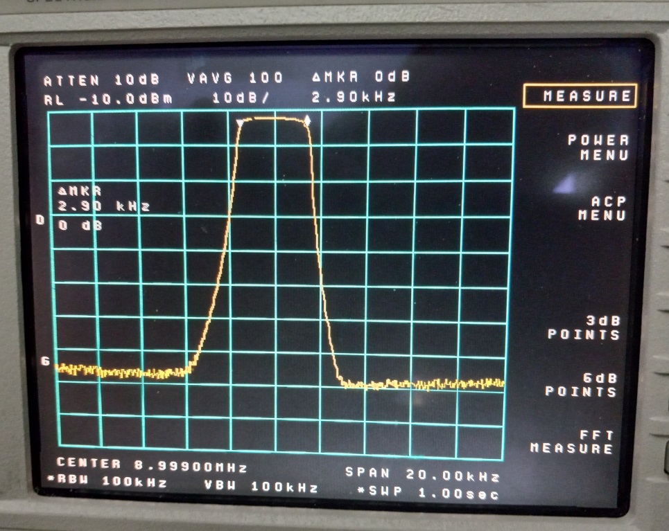
Finally, the -3 dB passband of the filter was measured with the spectrum analyzer. This measurement has been captured in Figure 9. The filter bandwidth is measured to be 2.9 kHz which compares favorably with the supplier’s measurement of 2.7 kHz although it is a bit wider than was hoped.
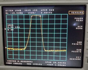
Figure 9. Crystal Filter 3 dB Passband Measurement. The bandwidth was reported by the supplier to be 2.7 kHz, but this measurement shows that it is 2.9 kHz. This is somewhat wider than was hoped, but this filter will be used. The steeper skirt at the high side of the response is characteristic of these filters. Please click on the figure to enlarge it.
Except for matching transformers, no alterations have been made to the filter other than to solder connectors to the PCB. The passband ripple is supposed to improve by bonding the crystals together with a soldered strap. From the results pictured, there doesn’t seem to be much utility in trying this. There is always the risk of damaging the filter by soldering to the crystal packages. The filter high side and low side skirt selectivities are as expected; the high side being steeper than the low side. Although this filter does not have skirts as steep as those found in a commercial SSB filter, it is adequate for this QRP rig.
Use of L-Matching Networks to Effect a Match
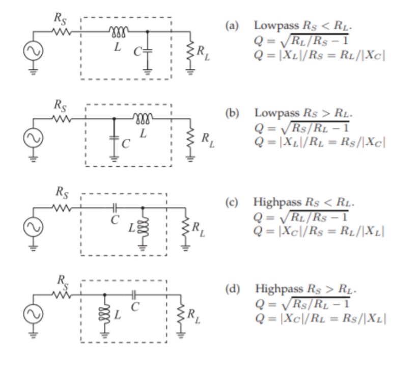
To demonstrate the method, the design of an L-matching network will be provided in this section. This same methodology has been used before in this blog[14]. For completeness, the topology choices are repeated in Figure 10.
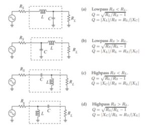
Figure 10. Topology Choices for L-Matching Networks. A topology is chosen depending upon whether a low-pass or high-pass configuration is required, and if Rs < RL , or if RS > RL . These topologies may be used to map and match the entire complex impedance plane. Reproduced under CC BY-NC by permission of Michael Steer, North Carolina State University. Please click on the figure to enlarge it.
The impedance level to which we wish to match, 160 ohms, is greater than the source impedance, 50 ohms, Rs < RL, and a solution topology (a) is selected, for the sake of example. It happens to be the low-pass topology that will pass DC current. This will place the inductor in series with the source and a capacitance in parallel with the crystal filter load impedance.
The shunt or parallel matching element, as it may be called, will always be closest to the larger of the two impedances. This mnemonic helps us to remember the topology choices. Whether the low-pass or high-pass topology is chosen will depend upon whether the component values are realizable, easily adjusted, and whether we want the network to pass DC current.
There is no need to design a different network for the filter output because the network is reciprocal meaning that it works the same way in reverse, and the mnemonic still applies. The output topology would be a shunt capacitor at the filter and a series inductor towards the load. You might prove this to yourself as an exercise by choosing the topology used for RS > RL since, this time, the high source impedance will be 160 ohms and the load impedance will be 50 ohms.
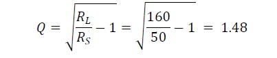
From Figure 10 (a) we have,
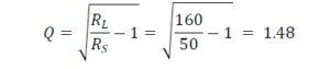
and
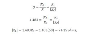
and
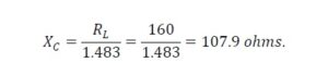
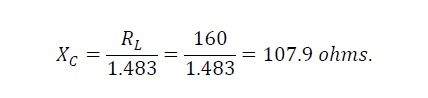
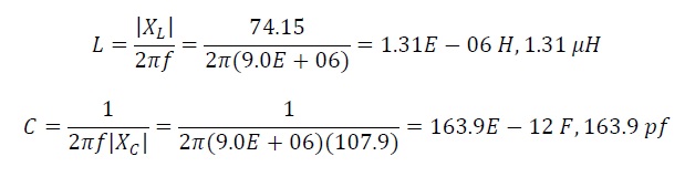
Solving for the values of the inductance and the capacitance, we have,
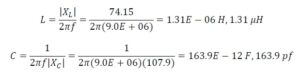
The matching network consists of a series inductance of 1.31 µH and a shunt capacitance of 163.9 pf.
Once you have mastered this process, you may wish to employ an online calculator[15].
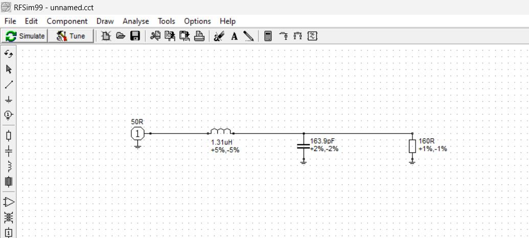
L-Network Simulation
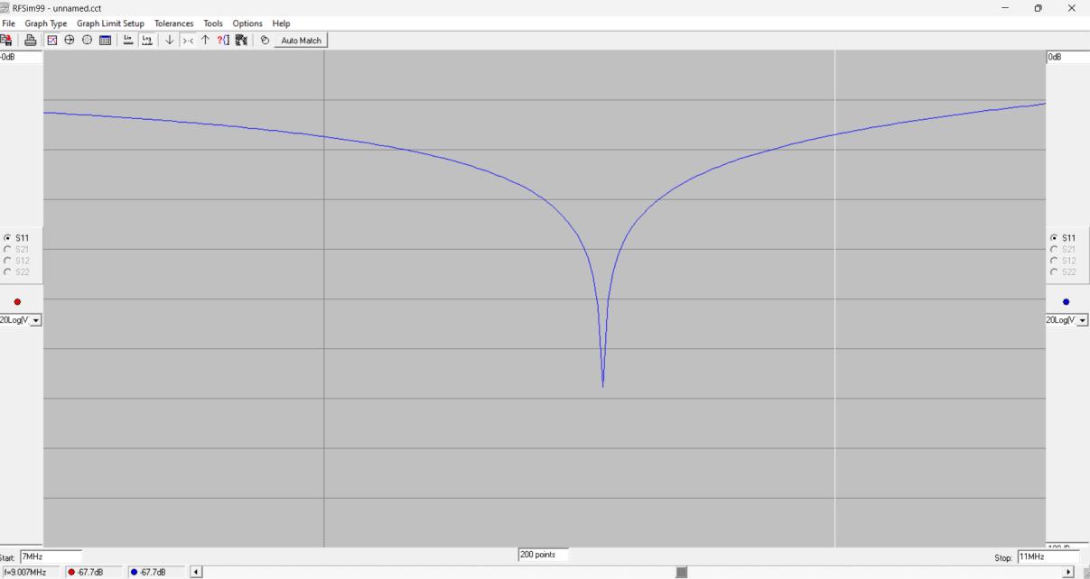
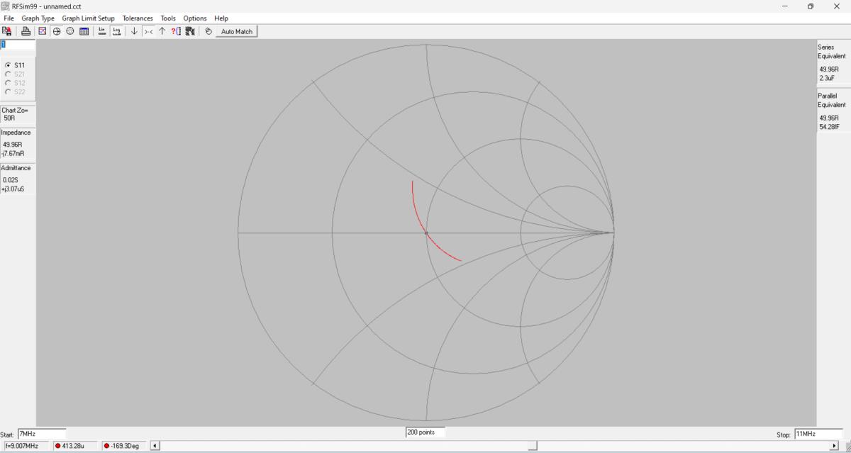
We can use RFSim99 to prove that we have achieved a match with this L-network. The model used for the simulation is shown in Figure 11. A rectangular plot of the return loss is shown in Figure 12. The Smith Chart of the match is shown in Figure 13.
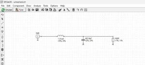
Figure 11. L-Matching Network Model. The 160-ohm input load impedance of the crystal filter can be matched to the 50-ohm source impedance with an L-network consisting of a series inductance of 1.31 µH and a shunt capacitance of 163.9 pf. Please click on the figure to enlarge it.
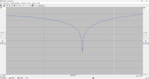
Figure 12. Return Loss of the L-Matching Network. The sweep is from 7 MHz to 11 MHz. The return loss for a very simple L-matching network at the design frequency of 9 MHz is better than 67 dB. Please click on the figure to enlarge it.
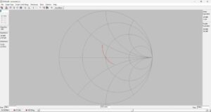
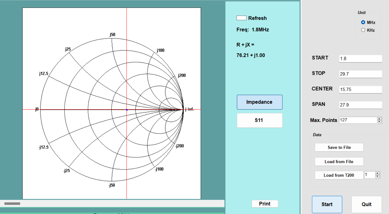
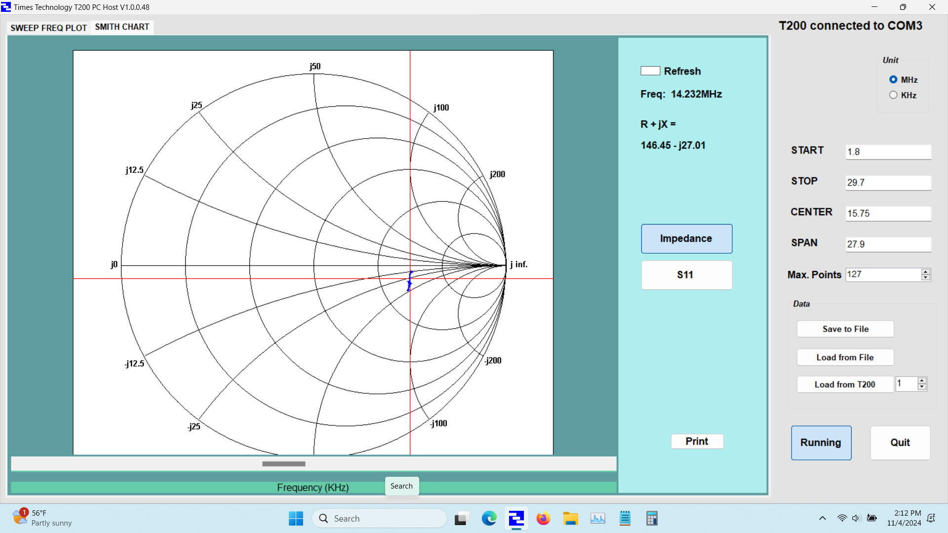
Figure 13. Smith Chart for the L-Matching Network. The sweep is from 7 MHz to 11 MHz. A perfect match is displayed on the Smith Chart at 9 MHz with the cursor positioned at the very center of the chart. Please click on the figure to enlarge it.
Conclusions
It has been demonstrated that matching to a crystal filter, commercial or homebrew, is not difficult. The techniques used for transformer and L-matching are ones that have been demonstrated previously. It is hoped that the reader will try both techniques for practice if only by following the examples that have been worked on.
References
[1] DigiKey, 701 Brooks Avenue South, Thief River Falls, MN.
[2] Milton Dishal, “Modern Network Theory Design of Single-Sideband Crystal Ladder Filters,” Proceedings of the IEEE, Sep 1965.
[3] Dishal Download: https://www.minikits.com.au/downloads
[4] Wes Hayward, Designing and Building Simple Crystal Filters, QST July 1987, pp. 24-29.
[5] Charlie Morris, ZL2CTM, https://www.youtube.com/watch?v=Ur7Cze-X0zo
[6] Jerry Hall, W0PWE, https://www.qsl.net/w0pwe/HB/Xtal_Osc.html
[7] Citizens Part Number HC-49/U-S9000000ABJB
[8] https://kitsandparts.com
[9] Ibid. https://kitsandparts.com/crystals.php
https://kitsandparts.com/XF.php
[10] Mostly DIY RF, https://mostlydiyrf.com/qer
[11] Fair Rite, PN 5943000201, https://fair-rite.com/product/toroids-5943000201/
[12] https://toroids.info/FT37-43.php
[13] James Butler, AD5GG, https://www.ad5gg.com/2017/04/06/free-rf-simulation-software/
[14] Martin Blustine, K1FQL, https://www.n1fd.org/2022/06/11/l-matching-networks/
[15] John Wetherell, author, Impedance Matching Network Designer, https://home.sandiego.edu/~ekim/e194rfs01/jwmatcher/matcher2.html